A Chiplet Interface Model for System-Level PPA Exploration By Austin Rovinski, New York University July 13, 2026
Zero trust in silicon: The new security imperative for chiplet-based 3D ICs By Tova Levy (Siemens) & Chris Jones (Crypto Quantique) July 2, 2026
Beyond the data pipe: Why connectivity IP is now the system-critical layer in every 3D IC By Tova Levy (Siemens EDA) & Archana Cheruliyil (Qualcomm) June 25, 2026
An Automated Interconnect Modeling Framework for Rapid Cryptolet Design Space Exploration By Austin Rovinski (NYU) June 24, 2026
DICE: Detailed Inter-Chiplet End-to-End PHY Modeling for Accurate Chiplet Simulation By Rashid Aligholipour June 22, 2026
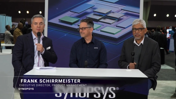
Blueprint for AI Hardware But with Instructions: Pre-Validated Chiplet Building Blocks By Synopsys, Arm, AMI May 28, 2026
Standardizing System-Level Interoperability for Multi-Vendor Chiplets By Gilberto Rodríguez, Openchip & Fady Dahoud, GSOC May 22, 2026
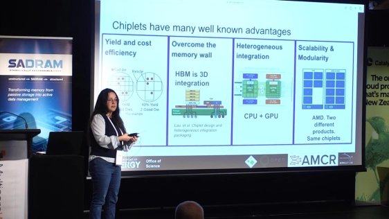
Towards wafer-scale optical interconnect relying on Silicon Photonics and advanced 3D assembly By Peter Ossieur May 20, 2026
Pre-Silicon Chiplet Verification for Datacenters By Ravi Narayanaswami, Cadence & Marc Meunier, Arm May 18, 2026
Cadence & Samsung: Chiplet Ecosystem Innovation for Edge AI | CadenceLive 2026 By Mick Posner, Cadence and Kevin Yee, Samsung Foundry May 2, 2026
Inside the AI Bottleneck: Data Movement, Chiplets, and System Scaling By Nandan Nayampally April 1, 2026
Advanced Semiconductor Packaging Explained: Hybrid Bonding, Chiplets & Manufacturing Innovation By TK Lee, Launch Tech March 25, 2026