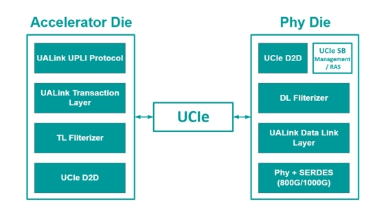
UALink over UCIe 3.0: Maximizing Performance for Chiplet-based Designs By Sriram Bhaskar Teja Mundru October 2, 2026
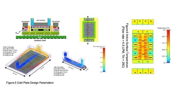
Ayar Labs and GUC Complete Successful Thermal Co-Simulation Testing of Co-Packaged Optics By Vladimir Stojanovic (Ayar Labs), Igor Elkanovich (GUC) October 2, 2026
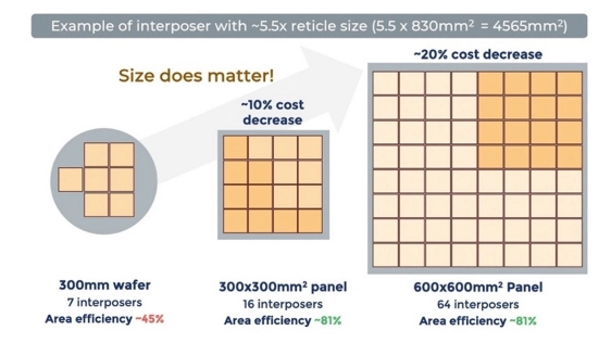
Overcoming Cleaning and Plating Challenges in Panel-Level Packaging and Manufacturing By ACM Research October 1, 2026
AMBA C2C: Moving forward with a converged AMBA foundation for C2C connectivity By Francisco Socal October 1, 2026
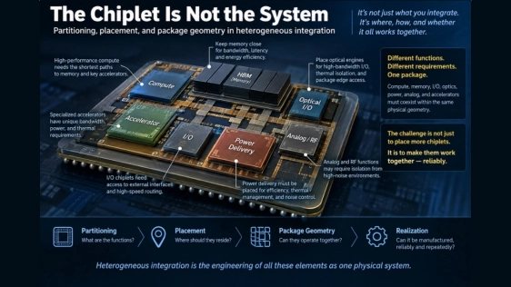
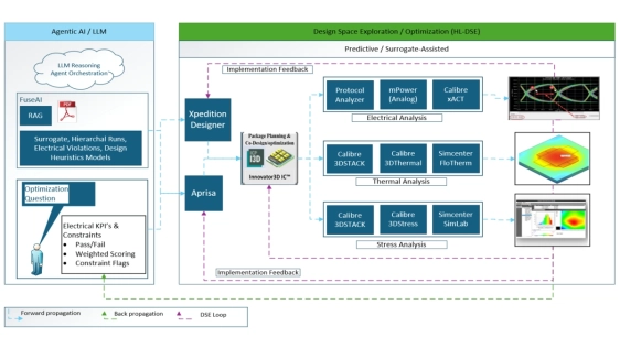
The Chiplet Is Not the System: Partitioning, Placement, and Package Geometry in Heterogeneous Integration By Moh Kolbehdari September 29, 2026
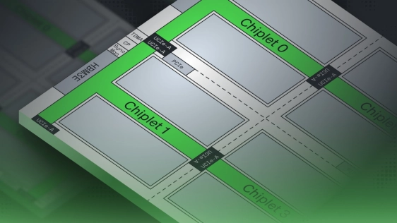
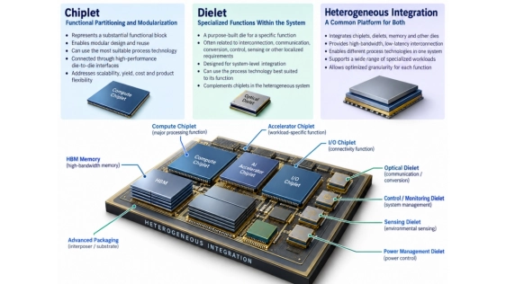
Chiplets and Dielets: Coexisting Technologies in Heterogeneous Integration By Moh Kolbehdari September 23, 2026
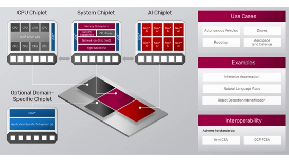
Accelerating Physical AI Through Cadence Silicon Solutions and Arm Total Design By Mick Posner September 22, 2026
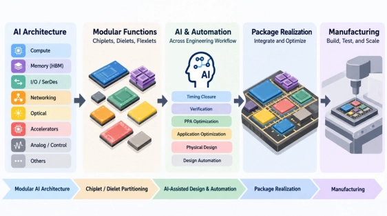
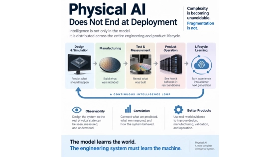
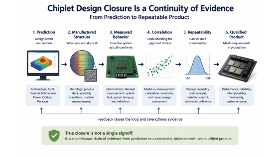
From Chiplet Design to Physical Reality: Why AI Hardware Needs Continuous Engineering Intelligence By Moh Kolbehdari September 16, 2026
Beyond the Die Boundary: How Arteris Multi-Die Technology Is Redefining AI System Design By Arteris September 10, 2026
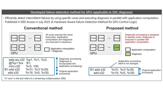
Riding the Tide Toward Open Ecosystem-Based Chiplet Integration―Hitachi’s Efforts to Overcome Industry-wide Challenges with Quality Improvement Technology By Kazumichi Moriyama September 7, 2026
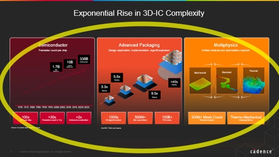
3D IC design for the AI era: an EDA perspective By Todd Burkholder, Sudarshan Deo, and Muhammad Hassan September 7, 2026
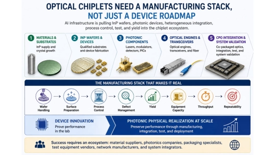
Optical Chiplets Need a Manufacturing Stack, Not Just a Device Roadmap By Moh Kolbehdari September 1, 2026