
The reference hub for the chiplet ecosystem
Where the chiplet marketplace starts with trust.
New Chiplets

Integrated voltage regulator (IVR) chiplet
- In-package voltage regulation for improved efficiency and performance.
- Reduced board-level complexity and external power components.
- Real-time control and feedback for dynamic system optimization.
High-performance connectivity chiplets
- PCIe and CXL-based connectivity for chiplet and system-level communications.
- High-bandwidth, low-latency data movement across compute, memory, and IO domains.
- Reusable IO architecture that reduces engineering effort across AI designs.

IMDD Tx PICs
- Reliable & qualified
- Supports single or dual input laser to drive all 8-channels
- CMOS-level drive voltage, featuring our patented ultra-low drive voltage design
- > 110 GHz electro-optic bandwidth

Near-Packaged Optics (NPO) Chiplet Solution
- CPO/NPO connectivity for GPU/Switch/ASIC with integrated OSPic™ all-optical signal processor
- High capacity, low latency up to 10Tbps for scale out CPO
- From 1.6Tbps to 6.4Tbps NPO in-field serviceability with heterogeneous laser integration
New Chiplet-Ready IP

Ncore Multi-Die Interconnect IP
- Scale Performance with Multi-Die Coherency
- Increase Bandwidth and Reduce Latency
- Tune Systems for Flexibility and Design Requirements

eFPGA Chiplet
- Optimized Performance for Advanced Computing
- Reduced Development Risk and Faster Time-to-Market
- MOSAICS-Ready Chiplet Architecture

High Performance Droplet
- High-Performance Analog Front-Ends (AFEs): Essential for data acquisition and signal processing in various applications.
- High-Speed Interfaces: Facilitating seamless communication between solutions. Omni Design supports various standards, including JESD204 and PCIe.
- Custom Solutions: Omni Design can tailor SoC solutions to meet specific customer requirements.

12nm EURYTION RFK1 - UCIe SP based Ka-Ku Band Chiplet Transceiver
- UCIe based Ka/Ku band transceiver
- Wide Bandwidth
- Scalable solution for dense mm-wave radio into single multi-chip modules
UCIe AP based 8-bit 170-Gsps Chiplet Transceiver
- 2T2R chiplet configuration
- 160/175-GSa/s sample rate
- 7-bit resolution

100G optical I/O chiplets
- RANOVUS®’ Odin® optical I/O cores set industry benchmarks for high bandwidth, low power consumption and small size for AI, cloud, metaverse, and communications applications
Insights
Ecosystem Highlights
PFN and SEMIFIVE Collaborate to Develop the MN-Core L2000 Series of Next-Generation AI Inference Chips
2026-11-17T06:34:00+00:00

Silicon Box semiconductor manufacturing facility in Italy enters Basic Design phase
2026-11-16T08:41:28+00:00
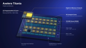
Axelera AI Unveils Titania Dual-Chiplet Architecture for AI Inference
2026-11-16T07:45:00+00:00
Expert Perspectives
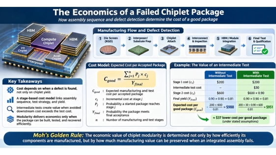
The Economics of a Failed Chiplet Package
November 17, 2026

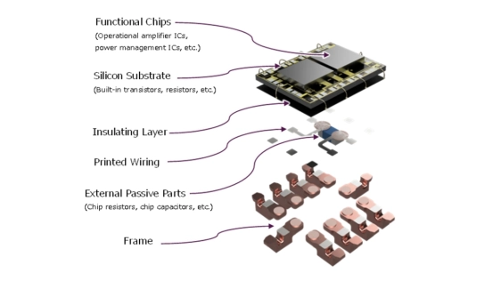
Silicon Motherboard Enables Double-Sided Integration of ICs and Passive Components
November 17, 2026

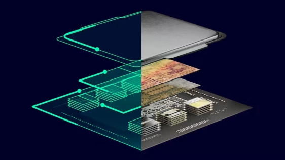
The Step-by-Step Process of STCO
November 16, 2026

The chip beneath the chips: Why silicon interposers matter more than ever
November 10, 2026

Recent Updates
Manufacturing & Supply Chain

Ecosystem & Strategy
HTSI & ficonTEC Strengthen Strategic Partnership to Expand Silicon Photonics Testing Capabilities
2026-11-17T14:32:00+00:00
Chiplet-Based Chips
PFN and SEMIFIVE Collaborate to Develop the MN-Core L2000 Series of Next-Generation AI Inference Chips
2026-11-17T06:34:00+00:00
Manufacturing & Supply Chain
Silicon Box semiconductor manufacturing facility in Italy enters Basic Design phase
2026-11-16T08:41:28+00:00
Chiplet-Based Chips
Axelera AI Unveils Titania Dual-Chiplet Architecture for AI Inference
2026-11-16T07:45:00+00:00
Ecosystem & Strategy
Technical Library
Whitepapers & Technical Articles
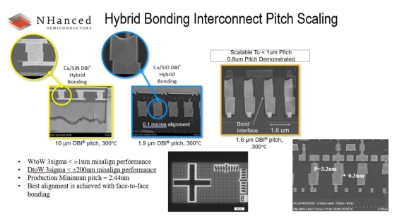
Technical Challenges for Ultra Fine Pitch Hybrid Bonding
November 17, 2026

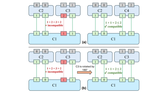
DT-MATCH: Defect- and Topology-Aware Chiplet Matching for Yield Optimization in Heterogeneous Integration
November 17, 2026

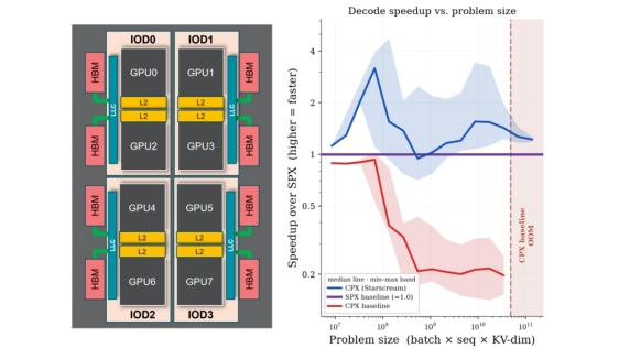
Starscream: Reimagining LLM Sharding on AMD Instinct GPUs with GPU Partitioning
November 13, 2026

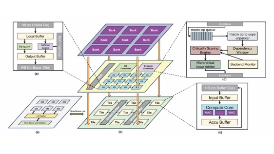
Tri-Stack-PIM: A Heterogeneous Multi-Die 3D-Integrated Processing-in-Memory Architecture for Efficient LLM Inference
November 11, 2026
Videos
The European Chip Ecosystem
November 10, 2026

Scaling up AI Compute, Memory and Connectivity

November 9, 2026

CURIE: A Cycle-Accurate and Synthesizable UCIe Interface for the Agile Design and Co-Simulation of Chiplets

Federated Chiplet Design and Simulation
November 6, 2026