Development and Optimization of Fine-Pitch RDL for RDL Interposer, and Embedded Bridge Die Interposer Fabrication Using Fan-Out Wafer-Level Packaging Technology
By Jung Won Lee 1, Sung Hyuk Lee 1, Jay Kim 1, Lewis Kang 1, Han Ju Yu 1, Min Ji Lee 1, Seong Hwan Han 1, Jae Kyung Lee 1, Hailey Hwang 1, Jun Gi Kim 1, Chan Young Hong 1, Jade Park 1, Su Hyun Kim 1, Myeong Jin Kim 2 and M. Kim 3
1 Advanced Technology Development Part, Technology Development Division, SEMI R&D Center, nepes Corporation, Republic of Korea
2 Technology Development Division, SEMI R&D Center, nepes Corporation, Republic of Korea
3 Department of Electronics Engineering, Kongju National University, Republic of Korea
Abstract
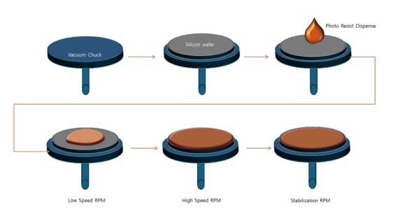
Chiplet technology enables the integration of heterogeneous dies into a single system, of-fering improved performance, scalability, and design flexibility. To support chiplet-based architectures, advanced packaging methods such as System-in-Package (SiP), 2.5D inter-posers, and 3D stacking are essential. A key enabler in these technologies is the fine-pitch Redistribution Layer (RDL), which ensures high interconnect density, signal integrity, and thermal efficiency. This study presents the development and optimization of fine-pitch RDL for two inter-poser types—2.5D RDL interposers and Embedded Bridge Die interposers—fabricated using fan-out wafer-level packaging (FOWLP). A newly developed positive photoresist was used in the photolithography process to define sub-micron RDL features. Process pa-rameters such as exposure energy and focus settings were systematically optimized to improve pattern resolution and structural integrity. Experimental results demonstrated that optimized lithographic conditions significantly enhanced the fidelity and uniformity of fine-pitch RDLs, enabling reliable signal trans-mission and manufacturability in multi-die systems. The findings confirm that fine-pitch RDL is a foundational technology for next-generation interposer solutions, supporting tighter die spacing and improved system performance. This technology can be imple-mented across various chiplet-based packaging platforms, such as those used in next generation artificial intelligence (AI) processors and high-performance computing (HPC) architectures.
Keywords: FOWLP (FanOut Wafer Level Package); interposer; chiplet; advanced packaging; fine pitch RDL
To read the full article, click here
Related Chiplet
- eFPGA Chiplet
- DPIQ Tx PICs
- IMDD Tx PICs
- Near-Packaged Optics (NPO) Chiplet Solution
- High Performance Droplet
Related Technical Papers
- ChipletQuake: On-die Digital Impedance Sensing for Chiplet and Interposer Verification
- Resister: A Resilient Interposer Architecture for Chiplet to Mitigate Timing Side-Channel Attacks
- Wafer Warpage of Silicon Interposer in Manufacturing Processes for High Density 2.5D Advanced Packaging: Causes, Measurement, Analysis and Optimization
- FAPlace: Joint Optimization of Chiplet Placement and Interposer Footprint for 2.5D Systems
Latest Technical Papers
- The Signal-Integrity Control Strategy of a TSV Array for a Chiplet-Based System
- ThermoDSE: A Thermal-Aware and Comprehensive Design Space Exploration for Chiplet-Based DNN Accelerators
- GPU-Accelerated Effective Resistance Analysis for 3D IC Power Delivery Network
- FAPlace: Joint Optimization of Chiplet Placement and Interposer Footprint for 2.5D Systems
- Chiplet-Escape: An Efficient Obstacle-Avoiding Escape Routing Method for Die-to-Die Interconnections in Chiplet-Based Designs