Advanced semiconductor packaging design via artificial intelligence and machine learning: A review
By Mohammad Rafiee, Pavas Saini
University of Ottawa, Canada
Abstract
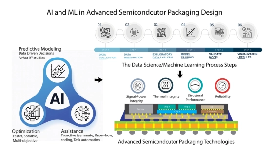
System performance now depends as much on advanced semiconductor packaging as on transistor scaling, especially with chiplets, 2.5D interposers, and 3D stacks. The resulting electro-thermal-mechanical coupling makes conventional electromagnetic (EM), finite-element (FEM), and computational fluid dynamics (CFD) analysis costly for design-space exploration. This review synthesizes how artificial intelligence (AI) and machine learning (ML) accelerate and augment packaging workflows across four domains—signal/power integrity (SI/PI), thermal integrity, structural/assembly behavior (warpage and stress), and reliability—and how AI and ML enables multi-physics co-design. We organize prior work by design role (surrogate modeling, design tuning, time-series tracking and multi objective co- design) and by algorithm family for fast surrogates; deep models (convolutional neural networks and long short-term memory networks) for images and waveforms; emerging reinforcement learning for routing, stack-up, and parameter auto-tuning; and physics-informed networks for thermally constrained settings. Cross-domain analysis reveals which models generalize broadly and which are specialized for data types or physics constraints. Remaining challenges for industrial adoption include reliance on simulation-only datasets, limited generalizability across architectures, incomplete uncertainty quantification, and interpretability concerns. We emphasize ongoing opportunities in integrating physics knowledge, uncertainty-aware learning, digital twin frameworks, transfer- and semi-supervised learning strategies, standardized benchmarking, and embedding AI and ML into electronic design automation (EDA) flows. Overall, AI and ML are advancing semiconductor packaging from simulation-driven iteration toward learning-augmented co-design, enabling more efficient, robust, and holistic optimization.
Keywords: AI/ML in advanced semiconductor packaging; Signal and power integrity; Thermal management; Package warpage and stress; Microelectronics reliability; Multi-physics co-design
To read the full article, click here
Related Chiplet
- eFPGA Chiplet
- DPIQ Tx PICs
- IMDD Tx PICs
- Near-Packaged Optics (NPO) Chiplet Solution
- High Performance Droplet
Related Technical Papers
- Material Needs and Measurement Challenges for Advanced Semiconductor Packaging: Understanding the Soft Side of Science
- Thermo-mechanical co-design of 2.5D flip-chip packages with silicon and glass interposers via finite element analysis and machine learning
- Intel Delivers Cutting-Edge Process Technologies to the Data Center with Intel 18A and Advanced Chiplet Packaging
- High-Bandwidth Chiplet Interconnects for Advanced Packaging Technologies in AI/ML Applications: Challenges and Solutions
Latest Technical Papers
- The Signal-Integrity Control Strategy of a TSV Array for a Chiplet-Based System
- ThermoDSE: A Thermal-Aware and Comprehensive Design Space Exploration for Chiplet-Based DNN Accelerators
- GPU-Accelerated Effective Resistance Analysis for 3D IC Power Delivery Network
- FAPlace: Joint Optimization of Chiplet Placement and Interposer Footprint for 2.5D Systems
- Chiplet-Escape: An Efficient Obstacle-Avoiding Escape Routing Method for Die-to-Die Interconnections in Chiplet-Based Designs