Interconnect Chiplet
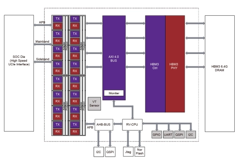
The ML100 IO Die is a high-bandwidth memory solution that integrates efficient UCIe (Die-to-Die) interconnect IP and HBM3 IP. The UCIe IP follows the UCIe 1.1 Specification and supports both standard and advanced packaging technologies, offering up to 1 TB/s of transfer bandwidth in a single module configuration. The UCIe supports the AXI4.0 interface standard, enabling ultra-low latency, high-speed interconnectivity between two dies. And the integrated HBM3 IP adheres to the HBM3 JESD238 standard and supports IO transfer rates of up to 6400 Mbps.
Additional data available! Features, portability, process node, and more can be viewed by logging in with your Chiplet Marketplace account.
- See the entire Interconnect Chiplet datasheet
- Get in contact with Interconnect Chiplet Supplier
Block Diagram
Related Chiplets
- Arm Compute Chiplet
- High-Density Electronic-Photonic Chiplet
- Speedcore eFPGA Chiplet
- Transceiver Chiplet
- Memory Chiplet
- 400G Transmitter Chiplet for 400G, 800G and 1.6T Pluggable Transceivers