AI silicon: Package becoming system architecture

The future of advanced packaging is not one universal package. It’s a technology platform capable of placing the right interconnect, material, die, memory stack, optical engine, and thermal structure at the right system boundary.
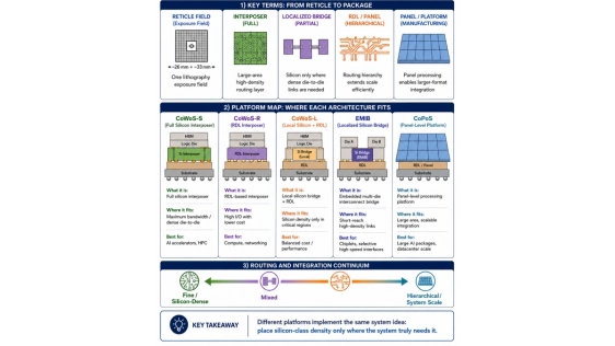 For many years, the design sequence appeared straightforward:
Design the chip → select the package → connect it to the board
That sequence is becoming less accurate. AI accelerators, high-bandwidth memory (HBM), chiplets, optical I/O, advanced cooling, and high-current power delivery are now so tightly coupled that the package can no longer be selected after the system architecture is largely complete.
The package increasingly determines:
- How the system can be partitioned
- How many chiplets can be integrated
- Where silicon-class interconnect density is required
- Where broader and lower-cost routing is sufficient
- How HBM is placed and connected
- Where electrical path should transition to optic
- How power reaches the compute elements
- How heat leaves the package
- How assembly can be manufactured, tested, repaired, and qualified
The package is no longer merely supporting the system. It’s defining what system can be built.
To read the full article, click here
Related Chiplet
- Optical Chiplet
- Reverse Gearbox Chiplet
- FlexGen Multi-Die Smart Network-on-Chip (NoC) IP
- Ncore Multi-Die Interconnect IP
- Integrated voltage regulator (IVR) chiplet
Related Blogs
- From Spec to Silicon: Successful Physical AI System Chiplet Bring-Up
- Chiplet Modularity Is Becoming Part of the AI Architecture
- Accelerating Physical AI Through Cadence Silicon Solutions and Arm Total Design
- Avoiding Multi-Die System Re-spins with New Early Architecture Exploration Technology