Advanced Packaging Changes the Rules for Semiconductor Health and Performance Management

In Other Words: How to Understand Every Chiplet Inside the System-in-Package
Systems-in-Package (SiPs) are enabling the next generation of Agentic and Physical AI across cloud, telecommunications, mobile, automotive and high-performance computing platforms. As infrastructure evolves from monolithic devices toward heterogeneous architectures, advanced packaging is becoming increasingly critical to achieving the required performance, bandwidth and power efficiency. But as processors, accelerators, memory and connectivity are brought together through increasingly sophisticated multi-die packages, managing each component in isolation is no longer enough.
A SiP is not simply a collection of individual dies. Once chiplets are integrated into the same package, new interactions emerge between them and with the package itself. Understanding those interactions requires visibility not only into each individual chiplet, but into how the chiplets behave together as a system.
Why a SiP Is Harder Than the Sum of Its Dies
Advanced packaging enables semiconductor companies to integrate more dies and increasingly heterogeneous components using technologies such as interposers, advanced substrates, through-silicon vias (TSVs), die stacking and high-bandwidth memory (HBM). These architectures provide enormous benefits, but they also introduce new electrical, thermal and mechanical interactions.
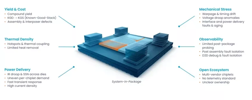
Challenges of systems-in-package
Power delivery becomes a system-level challenge. Different chiplets can have very different power demands, and activity on one die can influence the operating margins of another. IR drop, simultaneous switching noise, fast transients and shared power delivery networks can create voltage behavior that cannot be understood by looking at each chiplet independently.
Thermal behavior becomes increasingly coupled. High-power compute dies, HBM and other components are placed in close proximity, creating hotspots, thermal gradients and heat transfer between neighboring dies. In 3D architectures, heat removal becomes even more difficult as dies are vertically stacked and thermal paths become constrained.
Mechanical effects can become electrical effects. Warpage, package stress and thermo-mechanical effects introduced during assembly can alter timing and voltage margins. A die that behaved one way at wafer sort may behave differently after it has been bonded, stacked or integrated into the final package.
Yield economics become more challenging. A marginal die discovered at wafer sort is one problem. Discovering that same die after it has been integrated with an expensive interposer, substrate, HBM and other known-good components is a much more costly problem. Compound yield therefore becomes increasingly important as the number and value of components within the package increase.
And observability becomes harder just when it becomes more important. Once dies are assembled into a package, traditional probing becomes limited, fault isolation becomes more difficult and determining whether a problem originated in a chiplet, an interface, the package or an interaction between components can require significant debug effort.
Quality becomes harder to measure and assure. Advanced packaging introduces thousands of critical connections, including micro-bumps and other package interconnects, whose quality can be difficult to characterize directly. Marginal connections may pass conventional production tests yet contribute to degradation or failures later in the product lifecycle. When a system fails in production or returns from the field, determining whether the root cause lies in the chiplets, an interconnect or the package itself can be extremely difficult. This creates a need for measurable indicators of quality that can help identify marginalities early and track degradation over time.
Power delivery is one important example. As power traverses increasingly complex package structures and interconnects, and as the current density over these structures is ever increasing, the quality of the power-delivery path can directly affect voltage margin and system behavior. Different chiplets can have very different power demands, while IR drop, simultaneous switching noise, fast transients and shared power delivery networks can create effects that cannot be understood by looking at each chiplet independently. Even though power delivery is distributed over thousands of bumps, pads and through silicon vias (TSVs), a degradation of even one of them may cause a domino effect causing faster degradation of the neighboring pads.
The challenge is amplified further as the industry moves toward heterogeneous, multi-vendor chiplet ecosystems. No single die tells the whole story - and no single chiplet vendor necessarily has visibility into the complete package.
Shift Left: Know More Before You Package
The economics of advanced packaging make early decisions particularly valuable.
Conventional pass/fail testing at wafer sort may not reveal the parametric marginalities that become important after integration. For advanced packaging, that may not be enough. A die can pass conventional tests and still carry parametric marginalities that become important only after packaging.
Deep in-die measurements can provide another layer of information: how much timing margin exists, how a die responds to voltage variation, whether its parametric signature differs from its population and whether its behavior indicates increased sensitivity to the conditions it will experience after assembly.
This enables manufacturers to shift critical decisions left, before committing a die to an increasingly valuable package.
For example, telemetry-based advanced analytics and parametric deep data at wafer sort enable outlier detection beyond the industry’s best known methods, per-chiplet VDDmin prediction for static Voperational setting, and power/performance grading for chiplet mix-and-match. These insights can increase confidence in known-good-die quality and help prevent marginal dies from progressing into expensive downstream assembly.
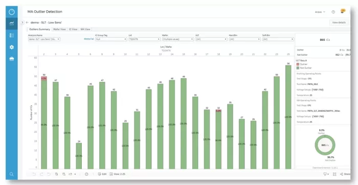
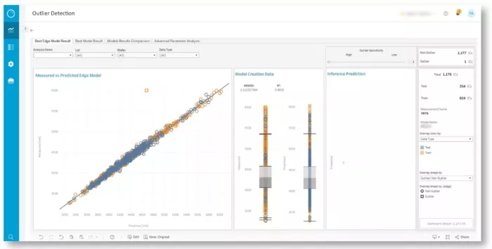
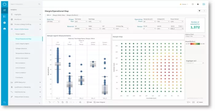
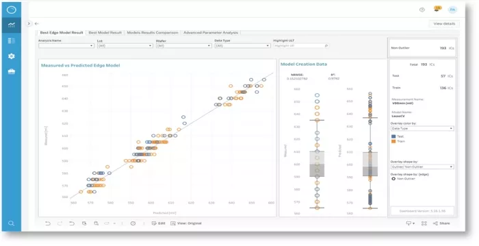
Advanced telemetry-based analytics for shift-left SiP production testing
The objective is no longer simply Known Good Die. It is increasingly:
Is this die ready to become part of this SiP?
That distinction can have a significant impact on compound yield, package scrap cost and final product quality.
What Changed Throughout Packaging?
Pre-packaging visibility is only one side of the problem.
Once a die has been integrated, manufacturers need to understand what has changed.
This is where pre-to-post packaging correlation becomes particularly valuable. By comparing parametric behavior before and after integration, changes associated with packaging can be identified and quantified.
A shift in timing margin, for example, may indicate an integration-induced effect rather than an intrinsic silicon defect. Changes in voltage behavior may point toward package power delivery. Spatial or die-to-die differences may correlate with thermal gradients, warpage or structural stress.
This becomes especially important across advanced packaging technologies such as interposers, substrates, HBM and TSV-based 3D stacks.
Instead of asking only:
“Does the assembled SiP pass?”
manufacturers can begin asking:
“What parameters changed when we packaged it? And why?”
That provides a much richer basis for package characterization, guard-band definition, root-cause analysis and production decisions.
From Individual Dies to Synchronized Inter-Chiplet Analysis
Post-packaging, the SiP increasingly needs to be treated as a system in its own right.
The behavior of one chiplet can affect another. A workload on a compute die can change package power demand, influence voltage droops, generate additional heat and affect timing margins elsewhere in the package. These interactions may also be transient, making static measurements insufficient.
Synchronized inter-chiplet analysis addresses this problem by analyzing measurements from multiple dies simultaneously and over time.
This enables engineers to correlate events across chiplets and investigate questions such as:
-
- Did a timing-margin shift on one chiplet coincide with a power event on another?
- Is a high temperature in one chiplet affecting the margin of a neighboring chiplet?
- Does a particular workload trigger correlated voltage or clock noise across multiple chiplets?
- Is an observed anomaly intrinsic to one die, or caused by an interaction within the package?
Time-series analysis adds another dimension by revealing transient instability and workload-dependent behavior that may not appear in static test results.
The result is a transition from per-chip monitoring toward package-aware analysis.
Multiple Data Streams, One View of the SiP
Advanced packaging also increases the number of relevant data sources.
Measurements originate from proteanTecs’ embedded monitors and sensors across multiple chiplets, in combination with manufacturing test equipment data and other third-party sources. Looking at these streams independently can miss the relationships between them.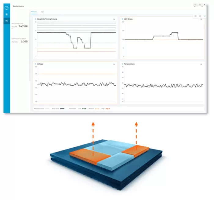
Example: Multi-die monitoring on proteanTecs’ SystemLens
Multi-stream analytics synchronizes and combines these measurements in the context of the complete SiP, allowing timing, voltage and thermal behavior to be correlated across chiplets, test stages and workload conditions.
This is particularly valuable when determining whether a problem originates in silicon, assembly, package power delivery, thermal interaction or workload behavior.
3D Integration Raises the Stakes Further
Many of these challenges become even more pronounced in 3D architectures.
Vertical stacking introduces additional dependencies around TSV integrity, thermo-mechanical stress, heat removal and vertical power delivery. It also creates the concept of a Known-Good-Stack (KGS) for 3D architectures, in addition to the traditional Known-Good-Die.
Testing and monitoring therefore need to move progressively through the stack lifecycle.
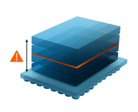
Before final packaging, stack-level testing helps identify interface issues, thermo-mechanical effects and TSV integrity problems. At final test, the fully assembled package can be validated under realistic conditions. During operation, the same embedded visibility can support monitoring of interface degradation and stack reliability over time.
The ability to maintain visibility through these stages becomes increasingly valuable because physical access decreases as integration increases.
From Production Visibility to In-Mission Awareness
The interactions created by advanced packaging do not stop when a SiP passes production test.
Workloads change. Temperatures change. Components age. And the guard-bands of different chiplets may evolve differently throughout the product lifetime. Interconnect quality can degrade as well. Continuous in-mission measurements can provide indicators of marginal or degrading package connections, helping distinguish interconnect-related issues from silicon, thermal or power-delivery effects when failures emerge over time. In-mission health and performance management therefore needs to become package-aware as well.
Thermal, power and timing awareness across the SiP can provide the context required to understand which chiplet is limiting system guard-bands at a particular point in time. Runtime applications can then use this information to support decisions around voltage, frequency, thermal management, health and reliability.
This is particularly important because SiP architectures can differ substantially. Some use centralized control through a primary chiplet; others distribute control functions. Power and clock domains may be shared or independent. Voltage regulators may be centralized or local, or even based on distributed Integrated Voltage Regulators (IVR) embedded into the package substrate.
There is no single control architecture for every SiP.
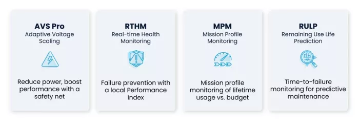
proteanTecs select applications for in-field health management, power reduction, and performance optimization.
To learn more about proteanTecs’ real-time, in-mission applications for chiplets and SiPs, schedule a demo today.
Health management and power reduction (or performance increase) therefore needs to adapt to the architecture of the package while evaluating the behavior of the complete system.
One Continuous View Across the SiP Lifecycle
The common thread across all of these challenges is visibility.
Before packaging, visibility helps determine whether a chiplet is truly ready for integration. After packaging, it helps determine what changed and how the chiplets are interacting. During production, it enables better screening, correlation, voltage setting and test decisions. And during in-mission operation, it provides the thermal, power, timing margin and health awareness required to optimize the complete SiP over its lifetime.
proteanTecs extends its deep data analytics and real-time health and performance monitoring and real time actuation capabilities across this lifecycle, combining an embedded Hardware Monitoring System with cloud, on-tester and real-time applications.
Together, these capabilities enable semiconductor and system companies to:
-
- Increase confidence in known-good-die and known-good-stack quality
- Shift critical decisions earlier in the manufacturing flow
- Improve visibility into package power delivery network and interconnect quality
- Improve compound yield and reduce costly package scrap
- Accelerate SiP characterization and root-cause analysis
- Optimize power and performance across multi-die systems
- Improve long-term health, reliability and lifecycle power/performance
As the industry moves toward increasingly heterogeneous and sophisticated multi-die architectures, the fundamental question is changing.
It is no longer enough to know whether each die works.
You need to know how every die is behaving, and how they are behaving together.
Related Chiplet
- Optical Chiplet
- Reverse Gearbox Chiplet
- FlexGen Multi-Die Smart Network-on-Chip (NoC) IP
- Ncore Multi-Die Interconnect IP
- Integrated voltage regulator (IVR) chiplet
Related Blogs
- Integrated Design Ecosystem™ for Chiplets and Heterogeneous Integration in Advanced Packaging Technology
- Tackling Key HBM and Advanced Packaging Bottlenecks for the AI Era
- Advanced Packaging Evolution: Chiplet and Silicon Photonics-CPO
- Stretching the antenna: Advanced antenna tuning with 9SW and SLATE™ advanced packaging technology on 9SW