Innovative FA hardware solution to enable system-level debug of 3D ICs
By Lesly Endrinal a,c, Jehan Saujauddin b, YuanChung Ho a, Dilbagh Singh a, Sasi Sekaran Sundaresan b, Vinod Kumar Kakumanu a, Jessen Gonzalez b, Willem D. van Driel c, G.Q. Zhang c
a Google LLC, 6420 Sequence Drive, San Diego, CA, 92126, United States of America
b Google LLC, 2015 Stierlin Ct, Mountain View, CA, 94043, United States of America
c Department of Microelectronics, Delft University of Technology, the Netherlands
Abstract
The rapid growth of generative Artificial Intelligence (AI), automotive electrification and Internet of Things (IoT) is driving an unprecedented demand for high-performance Integrated Circuits (ICs), projected to push the semiconductor industry to a $1 trillion business by 2030 (Burkacky et al., 2022; PWC, 2025). This drove the adoption of advanced process (FinFET, Gate-All-Around, Forksheet, CFET, Backside Power Delivery Network) and 3D package technologies (chiplets, Heterogeneous Integration, Co-packaged Optics). Unfortunately, component stacking in 3D ICs such as Package-on-Package (PoP) products creates an optical barrier during Electrical Fault Isolation (EFI).
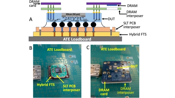
This paper presents a novel Failure Analysis (FA) hardware and sample preparation solution that enables System-Level FA on mobile System-on-a-Chip (SoC) PoP devices, where the DRAM is stacked atop the logic controller device. The primary challenge in performing EFI on the bottom die is providing direct line-of-sight (LoS) access while preserving the top DRAM functionality through extremely small interconnects called Through Interposer Vias (TIVs). For the first time, this groundbreaking hardware solution overcomes the challenge of connecting a DRAM atop the SoC silicon, utilizing the smallest possible interposer pin pitch (∼210 um) and advanced DRAM card design that incorporates stringent design rules to enable up to 6.3 Gbps using a DDR training test and runs standard Android stress applications. The results of the FA hardware solution for SLT platform will be discussed, together with several FA use cases that were enabled through this innovative solution. Lastly, this paper will discuss the limitations of this hardware, together with opportunities for improvement and further work.
This novel solution paves the way for the failure analysis of 3D IC devices on a system level platform, which are utilized not only in mobile applications, but also for cloud, server, and quantum computing ICs assembled in complex packages.
Keywords: 3D IC; Electrical Fault Isolation; Failure analysis; Interposer; Optical Fault Isolation; Package-on-Package; Photon Emission; SLT FA; System Level Test; System-on-a-Chip
To read the full article, click here
Related Chiplet
- Optical Chiplet
- Reverse Gearbox Chiplet
- FlexGen Multi-Die Smart Network-on-Chip (NoC) IP
- Ncore Multi-Die Interconnect IP
- Integrated voltage regulator (IVR) chiplet
Related Technical Papers
- GPU-Accelerated Effective Resistance Analysis for 3D IC Power Delivery Network
- Reliability challenges in 3D IC semiconductor design
- The multiphysics challenges of 3D IC designs
- TA3D: Timing-Aware 3D IC Partitioning and Placement by Optimizing the Critical Path
Latest Technical Papers
- Adaptive 3D Chiplet Architecture with Hybrid Wired–Wireless Interconnect for Energy-Efficient Heterogeneous Computing
- LLM-Augmented Bayesian Optimization with Adaptive Policies for Chiplet Design Space Exploration
- Divide and conquer: Scalable performance and energy in MCM GPUs
- A Composable AI-Accelerated Iterative Solver for 3D-IC Thermal Modeling
- QBX: A Compiler for 2-local Qubit Hamiltonian Simulation on Quantum Chiplets