The world’s first technology 'Silicon Motherboard' Circuits are formed on both sides of the silicon substrate, reducing mounting footprint by 80%
August 19, 2026 -- Nisshinbo Micro Devices Inc. has succeeded in establishing the world's first*1 3D mounting technology Silicon Motherboard (Si-MB®) that forms circuits on both sides of a silicon substrate, integrating ICs and passive components into one unit.
With this technology, we have achieved the integration of passive components, which was difficult for conventional chiplet technology, and in a prototype, the mounting footprint has been reduced by about 80% compared to conventional discrete configurations. Furthermore, by using the same package external shape as existing mass-produced one, we not only reduce the installation burden for customers but also accommodate applications requiring durability.
*1: Based on our research
Development Background
In recent years, the number of electronic components installed in industrial products, including industrial equipment, automotive devices, and communication devices, has been increasing due to the rise in functionality. This trend not only leads to increasing products size and transportation energy but also complicates the procurement and supply management of parts. To solve these issues, "component consolidation," which integrates multiple ICs and peripheral components, has been advancing. The three key elements in component consolidation are as follows.
- Versatility for mounting a wide variety of components, not limited to IC chips
- High-density implementation for miniaturization
- High durability for stable operation even under heavy load environments
Among these, chiplet technology is attracting attention as a technology that pursues miniaturization and high-density packaging. However, since chiplets are specialized for stacking IC chips, it is structurally difficult to install passive components such as chip resistors or capacitors. Additionally, as a trade-off for higher density, it is not highly durable and has limited application areas.
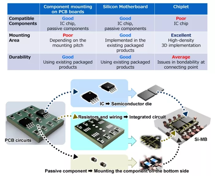
Figure 1: Issues of chiplet technology and overview of Silicon Motherboard
Features of Silicon Motherboard
Silicon Motherboard is a new high density mounting technology that combines the installation of passive components, which was difficult for conventional chiplet technology, with durability in high-load environments. Its internal structure is shown in Figure 2.
The main features of this technology are as follows:
- Functional chips mounted on the top surface of the silicon substrate
- Transistors, resistors, and capacitors elements are formed inside the substrate using wafer processing
- Mounting external passive components on the bottom side of the silicon substrate
Among these, the most distinctive feature is mounting external components on the bottom side of the silicon substrate. This makes it possible to incorporate passive components such as large-capacity capacitors (over 1,000 pF), low-resistance resistors (under 1 Ω), and inductors—which were difficult to install in conventional chiplets.
Furthermore, Silicon Motherboard does not require new special package shapes and adopts the existing mass-produced ones. As a result, users of Silicon Motherboard can leverage existing implementation equipment, significantly reducing implementation costs and evaluation periods.
Additionally, by adopting existing package shapes with mass production experience, making it applicable to applications ranging from consumer electronics to industrial and automotive applications requiring high reliability.
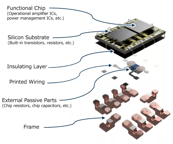
Figure 2: Structural diagram of Silicon Motherboard
Details of the Prototype
Figure 3 shows a prototype of Silicon Motherboard (function: window comparator). In this prototype, two comparator ICs are mounted as functional chips on a silicon substrate, and resistive elements are formed inside the substrate using wafer processing. Furthermore, two chip resistors are installed on the printed wiring underside of the silicon substrate.
As above, Silicon Motherboard is an advanced 3D mounting technology that integrates IC chips, built-in components using wafer processing, and external passive components. In this prototype, Silicon Motherboard technology reduced the mounting footprint by about 80% compared to conventional configurations. (Figure 4)
Our success in establishing Silicon Motherboard technology is backed by our expertise in analog IC technology, such as low noise and high precision. By leveraging such technology, we hold leading market shares*2 in the global op-amp, comparator, and LDO markets.
Analog ICs have characteristics that greatly affect their final performance not only by the IC itself, but also by the combination with peripheral components such as resistors, capacitors, and inductors, as well as by constant design. Therefore, optimizing the IC and peripheral components as an integrated unit is key to achieving higher performance.
However, with conventional chiplet technology, it is difficult to integrate passive components other than IC chips, and there were limitations in circuit design to maximize the performance of analog ICs.
Silicon Motherboard is a technology developed to solve this issue. This technology enables the integration of both IC chips and passive components, maximizing the performance of analog ICs.
Going forward, by utilizing this technology, we will expand not only to provide IC products but also to develop valuable system solutions including peripheral components. Through this, we will contribute to improving our customers' development efficiency and enhancing product performance.
*2: Marketing Eye Co., Ltd. Survey Results (2024)
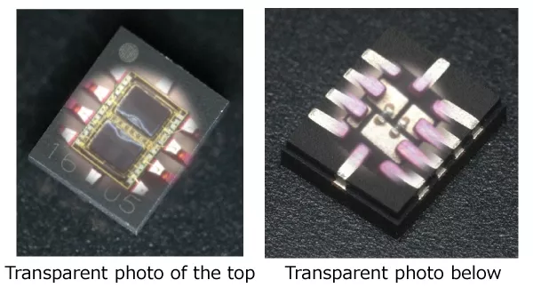
Figure 3: Prototype of Silicon Motherboard
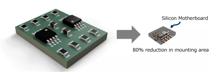
Figure 4: Example of component consolidation on Silicon Motherboard
This video provides an easy-to-understand overview of the key features of the Silicon Motherboard.
Related Chiplet
- Optical Chiplet
- Reverse Gearbox Chiplet
- FlexGen Multi-Die Smart Network-on-Chip (NoC) IP
- Ncore Multi-Die Interconnect IP
- Integrated voltage regulator (IVR) chiplet
Related News
- OKI Achieves 3D Integration of Thin-Film Analog ICs Using CFB Technology in Collaboration with Nisshinbo Micro Devices
- Saras Micro Devices Strengthens Senior Leadership Team to Scale Advanced Packaging Technology and Customer Growth
- CEA-Leti, CEA-List and PSMC Collaborate to Integrate RISC-V and MicroLED Silicon Photonics into 3D Stacking and Interposer for Next-Generation AI
- Lorentz Solution Jointly Presents with NVIDIA on Large-Scale 3D Terahertz EM Simulation for Real IC/3DIC Silicon Case Studies in Photonic Switches at 2025 TSMC OIP
Latest News
- Tenstorrent Releases Open Source Beta of the Open Chiplet Atlas® (OCA) Harness
- Building Out Advanced Packaging Portfolio, JCET Delivers Steady Revenue Growth and Improved Profitability in Q3 YTD 2026
- Egis Group and SiPearl Sign Strategic Cooperation and Investment Agreements to Expand Opportunities on a Global Scale
- Unigen Expands AI Module and Server Compute Collaboration to EdgeCortix RAIDEN Platform
- Amkor Technology and NVIDIA Advance Strategic Partnership for AI Infrastructure