Technical Challenges for Ultra Fine Pitch Hybrid Bonding
By Charles G. Woychik 1, Jonathan Abdilla 2, Chris Scanlan 2, Victor Vilar 1, Robert Patti 1, Dadi Setiadi 1, and Himanandhan Reddy Kottur 3, Navid Asadizanjani 3
1 NHanced Semiconductors, Inc.;
2 Besi Austria GmbH;
3 Department of Electrical and Computer Engineering, University of Florida
Abstract
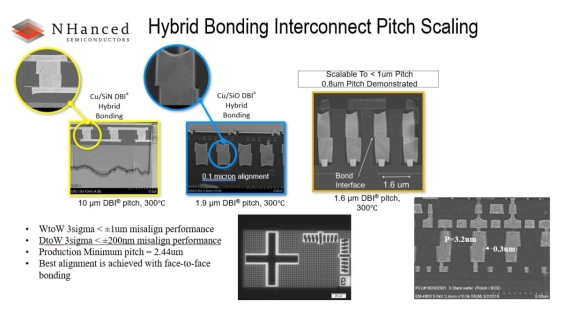
Hybrid bonding is rapidly emerging as a foundational technology for next-generation advanced packaging, enabling ultra-high-density interconnects required for heterogeneous integration of chiplets, logic, memory, and specialized accelerators. As the industry pushes toward ultra-fine pitch interconnects approaching single- digit microns and below, significant technical challenges must be addressed across the process flow. These challenges include achieving extremely tight wafer and die alignment tolerances, maintaining surface planarity and cleanliness at the nanometer scale, controlling copper dishing and dielectric erosion during CMP, and ensuring defect-free oxide and copper-copper bonding interfaces. In addition, scaling hybrid bonding to ultra-fine pitch requires improvements in metrology, defect inspection, thermal management, and yield control to support high-volume manufacturing. Integration with complementary technologies such as silicon interposers, wafer-to-wafer and die-to-wafer bonding architectures, and heterogeneous material stacks further increases process complexity. This presentation reviews the key technical barriers to ultra-fine pitch hybrid bonding and discusses emerging process solutions and equipment innovations required to enable reliable, high-density interconnects for future high-performance computing, AI, and advanced system-in- package applications.
Keywords: Hybrid bonding, AI enabled metrology, photonic electronic integration, optical interconnect
To read the full article, click here
Related Chiplet
- Optical Chiplet
- Reverse Gearbox Chiplet
- FlexGen Multi-Die Smart Network-on-Chip (NoC) IP
- Ncore Multi-Die Interconnect IP
- Integrated voltage regulator (IVR) chiplet
Related Technical Papers
- Probing the Nanoscale Onset of Plasticity in Electroplated Copper for Hybrid Bonding Structures via Multimodal Atomic Force Microscopy
- EOTPR Fine Pitch Probing for Die-to-Die Interconnect Failure Analysis
- Hybrid surface pre-treatments for enhancing copper-to-copper direct bonding
- Network Design for Wafer-Scale Systems with Wafer-on-Wafer Hybrid Bonding
Latest Technical Papers
- Technical Challenges for Ultra Fine Pitch Hybrid Bonding
- DT-MATCH: Defect- and Topology-Aware Chiplet Matching for Yield Optimization in Heterogeneous Integration
- Starscream: Reimagining LLM Sharding on AMD Instinct GPUs with GPU Partitioning
- Tri-Stack-PIM: A Heterogeneous Multi-Die 3D-Integrated Processing-in-Memory Architecture for Efficient LLM Inference
- CU-3D: A Scalable Legality-Aware RTL-to-GDS Flow for 3D-IC Physical Design