Probing the Nanoscale Onset of Plasticity in Electroplated Copper for Hybrid Bonding Structures via Multimodal Atomic Force Microscopy
By Nicolas A. Alderete 1,2, Paresh D. Daharwal 3, Cristian V. Ciobanu 4, and Gheorghe Stan 1
1 Material Measurement Laboratory, National Institute of Standards and Technology, Gaithersburg, Maryland 20899, United States
2 School of Science and Engineering, The George Washington University, Washington, D.C. 20052, United States
3 Advanced Packaging Technology and Manufacturing, Intel Corporation, Hillsboro, Oregon 97124, United States
4 Department of Mechanical Engineering and Materials Science Program, Colorado School of Mines, Golden, Colorado 80401, United States
Abstract
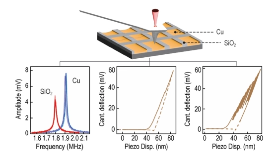
The slowdown of Moore’s law has elicited a paradigm shift whereby shrinking of in-plane dimensions is being replaced by 3D-stacking advanced packaging approaches to satisfy the ever-increasing demands for power, performance, area, and cost. Driven by the widespread use of metallic interconnects with submicron pitches, robust metrology for probing mechanical behavior at the nanoscale emerges as a key area of interest in the semiconductor industry. Here, we develop an atomic force microscopy (AFM)-based protocol for characterizing the incipient stages of plasticity and illustrate it on hybrid bonding-ready (prior to bonding) copper pads. We combined AFM’s high-resolution imaging with contact resonance and indentation techniques (including single- and multistep indentation) to characterize the mechanical heterogeneity of the material, quantify the nanoscopic yield stress statistics, and derive indentation stress–strain curves. From these measurements, we have clarified the mechanisms of early plasticity and determined the elastoplastic constitutive response of polycrystalline copper, including parameters such as elastic modulus, yield stress, and strain-hardening slope. Besides providing metrology relevant to various length scales, our approach offers a pathway to utilize an industry-standard instrument for characterizing the thermomechanical properties that are essential for the development of semiconductor structures.
To read the full article, click here
Related Chiplet
- Integrated voltage regulator (IVR) chiplet
- High-performance connectivity chiplets
- eFPGA Chiplet
- DPIQ Tx PICs
- IMDD Tx PICs
Related Technical Papers
- Revamping the Semiconductor Industry with Hybrid Bonding
- Thermal Issues Related to Hybrid Bonding of 3D-Stacked High Bandwidth Memory: A Comprehensive Review
- Hybrid Bonding With Polymeric Interlayer Dielectric Layers Patterned by Nanoimprint Lithography
- Hybrid surface pre-treatments for enhancing copper-to-copper direct bonding
Latest Technical Papers
- AI-Driven Thermal Mapping and Management in 3D Integrated Photonic Circuits
- CLIP-3D: Closed-Loop Evaluation of Performance and Physical Constraints for 3D ICs
- StreamDQ: Near-Memory Weight DeQuantization in Custom HBM for Scalable AI Inference Acceleration
- HCRMap: Pressure-Aware Hot-Expert Residency Mapping for 3.5D MoE Chiplet Inference
- Chiplet3D: Pin- and Thermal-Aware 3D Chiplet Floorplanning via Convolution-Embedded MILP