Network Design for Wafer-Scale Systems with Wafer-on-Wafer Hybrid Bonding
By Patrick Iff, Tommaso Bonato, Maciej Besta, Luca Benini, Torsten Hoefler
ETH Zurich
Abstract
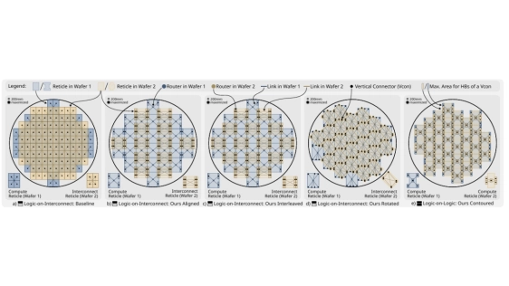
Transformer-based large language models are increasingly constrained by data movement as communication bandwidth drops sharply beyond the chip boundary. Wafer-scale integration using wafer-on-wafer hybrid bonding alleviates this limitation by providing ultra-high bandwidth between reticles on bonded wafers. In this paper, we investigate how the physical placement of reticles on wafers influences the achievable network topology and the resulting communication performance. Starting from a 2D mesh-like baseline, we propose four reticle placements (Aligned, Interleaved, Rotated, and Contoured) that improve throughput by up to 250%, reduce latency by up to 36%, and decrease energy per transmitted byte by up to 38%.
To read the full article, click here
Related Chiplet
- Integrated voltage regulator (IVR) chiplet
- High-performance connectivity chiplets
- eFPGA Chiplet
- DPIQ Tx PICs
- IMDD Tx PICs
Related Technical Papers
- Revamping the Semiconductor Industry with Hybrid Bonding
- Hybrid Bonding With Polymeric Interlayer Dielectric Layers Patterned by Nanoimprint Lithography
- PICNIC: Silicon Photonic Interconnected Chiplets with Computational Network and In-memory Computing for LLM Inference Acceleration
- Probing the Nanoscale Onset of Plasticity in Electroplated Copper for Hybrid Bonding Structures via Multimodal Atomic Force Microscopy
Latest Technical Papers
- AI-Driven Thermal Mapping and Management in 3D Integrated Photonic Circuits
- CLIP-3D: Closed-Loop Evaluation of Performance and Physical Constraints for 3D ICs
- StreamDQ: Near-Memory Weight DeQuantization in Custom HBM for Scalable AI Inference Acceleration
- HCRMap: Pressure-Aware Hot-Expert Residency Mapping for 3.5D MoE Chiplet Inference
- Chiplet3D: Pin- and Thermal-Aware 3D Chiplet Floorplanning via Convolution-Embedded MILP