Micro-Transfer Printing on Silicon Photonics: Tutorial, Recent Progress and Outlook
By Ye Chen et al.
Ghent University, imec
Abstract
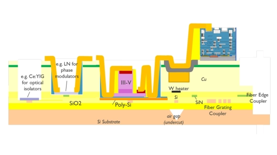
This paper highlights micro-transfer printing (MTP) as a promising scalable approach to heterogeneous integration for silicon photonics. MTP uniquely achieves high integration density, high throughput, and high material efficiency through a low-temperature, back-end integration process. Current demonstrations, including integrated III-V lasers and thin-film electro-optic modulators, confirm MTP's potential. Industrial adoption requires resolving challenges related to final integration yield and throughput, device reliability, and supply chain maturity.
Index Terms — Silicon Photonics, Heterogeneous Integration, Micro-Transfer Printing
To read the full article, click here
Related Chiplet
- Optical Chiplet
- Reverse Gearbox Chiplet
- FlexGen Multi-Die Smart Network-on-Chip (NoC) IP
- Ncore Multi-Die Interconnect IP
- Integrated voltage regulator (IVR) chiplet
Related Technical Papers
- The Evolution of Photonic Integrated Circuits and Silicon Photonics
- Quantum Dot DBR Lasers Monolithically Integrated on Silicon Photonics by In-Pocket Heteroepitaxy
- A 3D-integrated BiCMOS-silicon photonics high-speed receiver realized using micro-transfer printing
- On hardware security and trust for chiplet-based 2.5D and 3D ICs: Challenges and Innovations
Latest Technical Papers
- Adaptive 3D Chiplet Architecture with Hybrid Wired–Wireless Interconnect for Energy-Efficient Heterogeneous Computing
- LLM-Augmented Bayesian Optimization with Adaptive Policies for Chiplet Design Space Exploration
- Divide and conquer: Scalable performance and energy in MCM GPUs
- A Composable AI-Accelerated Iterative Solver for 3D-IC Thermal Modeling
- QBX: A Compiler for 2-local Qubit Hamiltonian Simulation on Quantum Chiplets