Quantum Dot DBR Lasers Monolithically Integrated on Silicon Photonics by In-Pocket Heteroepitaxy
By Rosalyn Koscica 1, Alec Skipper 1, Bei Shi 1, Kaiyin Feng 1, Gerald Leake 2 and Michael Zylstra 3
1 University of California, USA
2 RF SUNY Polytechnic Institute, USA
3 Analog Photonics, USA
Abstract:
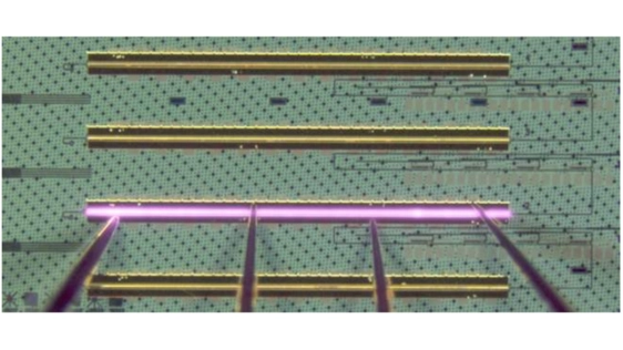
Monolithically integrated lasers on silicon photonics enable scalable, foundry-compatible production for data communications applications. However, material mismatches in heteroepitaxial systems and high coupling losses pose challenges for III-V integration on silicon. We combine three techniques: recessed silicon pockets for III-V growth, two-step heteroepitaxy using both MOCVD and MBE, and a polymer facet gap-fill approach to develop O-band InAs quantum dot lasers monolithically integrated on silicon photonics chiplets. Lasers coupled to silicon ring resonators and silicon nitride distributed Bragg reflectors (DBR) demonstrate single-mode lasing with side-mode suppression ratio up to 32 dB. Devices lase at temperatures up to 105 °C with an extrapolated operational lifetime of 6.2 years at 35 °C.
Index Terms—Active-passive coupling, DBR laser, III-V on Si integration, monolithic integration, optical coupling, O-band, quantum dot laser, semiconductor laser, silicon photonics.
To read the full article, click here
Related Chiplet
- Integrated voltage regulator (IVR) chiplet
- High-performance connectivity chiplets
- eFPGA Chiplet
- DPIQ Tx PICs
- IMDD Tx PICs
Related Technical Papers
- Micro-Transfer Printing on Silicon Photonics: Tutorial, Recent Progress and Outlook
- The Evolution of Photonic Integrated Circuits and Silicon Photonics
- Foundry-Enabled Patterning of Diamond Quantum Microchiplets for Scalable Quantum Photonics
- Interfacing silicon photonics for high-density co-packaged optics
Latest Technical Papers
- APEX: an Adaptive Photonic-Electronic Chiplet Interconnection Architecture for DNN Inference
- Formal Foundations for Known Good Reliable Die Screening in Chiplet-Based AI Systems-on-Chip
- Optimization of Test-Access Architectures and Test Scheduling for 2.5D/3D Integration
- Learning to Place Chiplets: A Multi-Objective Reinforcement Learning Approach
- ThAME: 3D Memory-Enabled Heterogeneous Accelerator for LLM Mixture of Experts