A 3D-integrated BiCMOS-silicon photonics high-speed receiver realized using micro-transfer printing
By Ye Gu 1, He Li 2, Tinus Pannier 1, Shengpu Niu 1, Patrick Heise 3,4, Christian Mai 3, Prasanna Ramaswamy 5, Alex Farrel 5, Alin Fecioru 5, Antonio Jose Trindade 5, Ruggero Loi 5, Nishant Singh 1, Senbiao Qin 2, Biwei Pan 2, Jing Zhang 2, Johanna Rimbock 6, Kristof Dhaenens 7, Toon De Baere 7, Geert Van Steenberge 7, Dieter Bode 8, Dimitrios Velenis 8, Guy Lepage 8, Neha Singh 8, Joris Van Campenhout 8, Xin Yin 1, Gunther Roelkens 2, Peter Ossieur 1
1 IDLab, INTEC, Ghent University – imec, Ghent, 9052, Belgium.
2 Photonics Research Group, INTEC, Ghent University– imec, Ghent, 9052, Belgium.
3 IHP- Leibniz-Institut fur innovative Mikroelektronik, Frankfurt (Oder), Germany.
4 Technical University of Applied Sciences Mittelhessen, Gießen, 35390, Germany.
5 X-Celeprint Ltd., Lee Maltings, Dyke Parade, Cork, Ireland.
6 EV Group, E. Thallner GmbH, St. Florian am Inn,Austria.
7 Center for Microsystems Technology (CMST), INTEC, imec– Ghent University, Ghent, 9052, Belgium.
8 imec, Kapeldreef 75, Leuven, 3001, Belgium.
Abstract
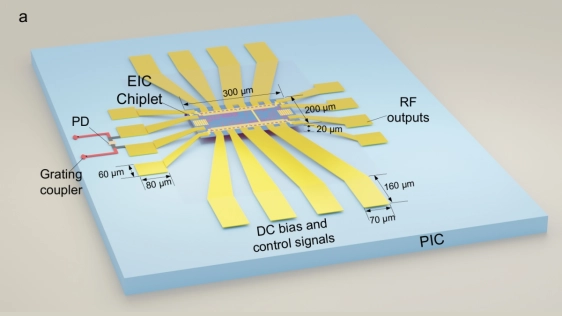
Meeting the escalating demands of data transmission and computing, driven by artificial intelligence (AI), requires not only faster optical transceivers but also advanced integration technologies that can seamlessly combine photonic and elec tronic components. Traditional approaches struggle to overcome the parasitic limitations arising from fabricating those components using different processes. Here, we report a novel 3D heterogeneously integrated optical receiver based on micro-transfer printing (µTP), enabling the co-integration of a compact bipolar CMOS(BiCMOS) electronic chiplet (0.06 mm2) directly onto a silicon photonic integrated circuit (SiPIC). While previous µTP demonstrations have focused primarily on photonic integration, our work pioneers the direct integration of electronics and photonics, significantly enhancing performance and scalability. The resulting optical receiver achieves 224 Gb/s four-level pulse amplitude mod ulation (PAM-4) operation, delivering-5.2 dBm optical modulation amplitude (OMA) sensitivity at a bit-error rate (BER) of 2.4×10⁻⁴, a record-small foot print, and an excellent power efficiency of 0.51 pJ/b. This demonstration not only showcases the potential of µTP for high-density, cost-efficient integration but also represents a critical step toward next-generation optical interconnects in the AI era.
Keywords: Heterogeneous integration, micro-transfer printing, silicon photonics, SiGe BiCMOS, optical receivers
To read the full article, click here
Related Chiplet
- Optical Chiplet
- Reverse Gearbox Chiplet
- FlexGen Multi-Die Smart Network-on-Chip (NoC) IP
- Ncore Multi-Die Interconnect IP
- Integrated voltage regulator (IVR) chiplet
Related Technical Papers
- Micro-Transfer Printing on Silicon Photonics: Tutorial, Recent Progress and Outlook
- ChipAI: A scalable chiplet-based accelerator for efficient DNN inference using silicon photonics
- Recent Progress in Structural Integrity Evaluation of Microelectronic Packaging Using Scanning Acoustic Microscopy (SAM): A Review
- Plasma Etch Process Optimization for Photonic-Grade Diamond-on-Insulator Substrates and Thickness Evaluation using Colorimetry
Latest Technical Papers
- Adaptive 3D Chiplet Architecture with Hybrid Wired–Wireless Interconnect for Energy-Efficient Heterogeneous Computing
- LLM-Augmented Bayesian Optimization with Adaptive Policies for Chiplet Design Space Exploration
- Divide and conquer: Scalable performance and energy in MCM GPUs
- A Composable AI-Accelerated Iterative Solver for 3D-IC Thermal Modeling
- QBX: A Compiler for 2-local Qubit Hamiltonian Simulation on Quantum Chiplets