Tiny Chiplets Enabled by Packaging Scaling: Opportunities in ESD Protection and Signal Integrity
By Emad Haque 1, Pragnya Sudershan Nalla 2, Jeff Zhang 1, Sachin S. Sapatnekar 2, Chaitali Chakrabarti 1 and Yu Cao 2
1 School of Electrical, Computer and Energy Engineering, Arizona State University, Tempe, AZ 85282, USA
2 Department of Electrical and Computer Engineering, University of Minnesota, Minneapolis, MN 55455, USA
Abstract
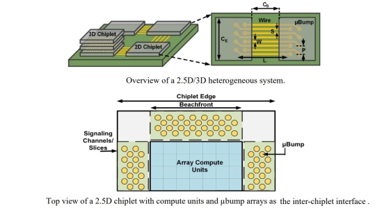
The scaling of advanced packaging technologies provides abundant interconnection resources for 2.5D/3D heterogeneous integration (HI), thereby enabling the construction of larger-scale VLSI systems with higher energy efficiency in data movement. However, conventional I/O circuitry, including electrostatic discharge (ESD) protection and signaling, introduces significant area overhead. Prior studies have identified this overhead as a major constraint in reducing chiplet size below 100 mm2. In this study, we revisit reliability requirements from the perspective of chiplet interface design. Through parasitic extraction and SPICE simulations, we demonstrate that ESD protection and inter-chiplet signaling can be substantially simplified in future 2.5D/3D packaging technologies. Such simplification, in turn, paves the road for further chiplet miniaturization and improves the composability and reusability of tiny chiplets.
To read the full article, click here
Related Chiplet
- Integrated voltage regulator (IVR) chiplet
- High-performance connectivity chiplets
- eFPGA Chiplet
- DPIQ Tx PICs
- IMDD Tx PICs
Related Technical Papers
- Signal Integrity Challenges in Chiplet-Based Designs: Addressing Performance and Security
- Recent Progress in Structural Integrity Evaluation of Microelectronic Packaging Using Scanning Acoustic Microscopy (SAM): A Review
- A physics-constrained and data-driven approach for thermal field inversion in chiplet-based packaging
- Toward Digital Twins in 3D IC Packaging: A Critical Review of Physics, Data, and Hybrid Architectures
Latest Technical Papers
- APEX: an Adaptive Photonic-Electronic Chiplet Interconnection Architecture for DNN Inference
- Formal Foundations for Known Good Reliable Die Screening in Chiplet-Based AI Systems-on-Chip
- Optimization of Test-Access Architectures and Test Scheduling for 2.5D/3D Integration
- Learning to Place Chiplets: A Multi-Objective Reinforcement Learning Approach
- ThAME: 3D Memory-Enabled Heterogeneous Accelerator for LLM Mixture of Experts