Recent Progress in Structural Integrity Evaluation of Microelectronic Packaging Using Scanning Acoustic Microscopy (SAM): A Review
By Pouria Meshki Zadeh 1 , Sebastian Brand 2 and Ehsan Dehghan-Niri 1
1 School of Manufacturing Systems and Networks, Ira A. Fulton Schools of Engineering, Arizona State University, Mesa, AZ 85212, USA
2 Fraunhofer Institute for Microstructure of Materials and Systems IMWS, Walter-Hülse-St., 06120 Halle, Germany
Abstract
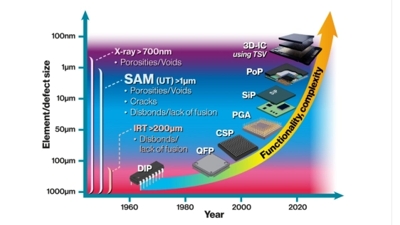
Microelectronic packaging is crucial for protecting, powering, and interconnecting semiconductor chips, playing a critical role in the functionality and reliability of electronic devices. With the growth in complexity and miniaturization of these products, the implementation of efficient inspection techniques becomes crucial in preventing failures that may result in device malfunctions. This review paper examines the progress made in utilizing Scanning Acoustic Microscopy (SAM) to assess the structural integrity of microelectronic systems within the broader field of Nondestructive Evaluation/Testing (NDE/T) methods. With an exclusive emphasis on SAM, we point out SAM technological advancements in multidie stacking, Through Silicon Vias (TSV), and hybrid bonding inspection that improve inspection sensitivity and resolution required to be prepared for upcoming challenges accompanying 3D- and heterogeneous integration architectures. Some of these approaches compromise the depth of inspection for the benefit of lateral resolution, while others do not sacrifice the in-depth range of evaluation. These developments are of the utmost importance in addressing the substantial obstacles associated with examining microelectronic packages, facilitating the early detection of potential failures, and enhancing the reliability and robustness of semiconductor devices. Furthermore, our discussion consists of the fundamental principles and practical approaches of SAM. It also examines recent investigations that integrate SAM with machine learning concepts and the application of deep learning models in order to automate defect detection and characterization, thus substantially augmenting the efficiency of microelectronic package assessments.
Keywords: microelectronic packaging; semiconductors; nondestructive evaluation; heterogeneous packages; 3D-ICs; artificial intelligence; Scanning Acoustic Microscope
To read the full article, click here
Related Chiplet
- Integrated voltage regulator (IVR) chiplet
- High-performance connectivity chiplets
- eFPGA Chiplet
- DPIQ Tx PICs
- IMDD Tx PICs
Related Technical Papers
- Probing the Nanoscale Onset of Plasticity in Electroplated Copper for Hybrid Bonding Structures via Multimodal Atomic Force Microscopy
- Small Dies, Big Dreams: Challenges and Opportunities in Chiplet Commoditization
- An Introduction to Direct RF Sampling in a World Evolving Towards Chiplets – Part 1
Latest Technical Papers
- APEX: an Adaptive Photonic-Electronic Chiplet Interconnection Architecture for DNN Inference
- Formal Foundations for Known Good Reliable Die Screening in Chiplet-Based AI Systems-on-Chip
- Optimization of Test-Access Architectures and Test Scheduling for 2.5D/3D Integration
- Learning to Place Chiplets: A Multi-Objective Reinforcement Learning Approach
- ThAME: 3D Memory-Enabled Heterogeneous Accelerator for LLM Mixture of Experts