Thermal Implications of Non-Uniform Power in BSPDN-Enabled 2.5D/3D Chiplet-based Systems-in-Package using Nanosheet Technology
By Yukai Chen 1, Massimiliano Di Todaro 1,3, Bjorn Vermeersch 1, Herman Oprins 1, Daniele Jahier Pagliari 3, Julien Ryckaert 1, Dwaipayan Biswas 1 and James Myers 2
1 IMEC, Belgium
2 IMEC, United Kingdom
3 DAUIN, Politecnico di Torino, Italy
Abstract
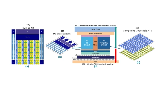
Advances in nanosheet technologies have significantly increased power densities, exacerbating thermal management challenges in 2.5D/3D chiplet-based Systems-in-Package (SiP). While traditional thermal analyses often employ uniform power maps to simplify computational complexity, this practice neglects localized heating effects, leading to inaccuracies in thermal estimations, especially when comparing power delivery networks (PDN) in 3D integration. This work examines the thermal impact of non-uniform power distributions on SiPs utilizing frontside (FSPDN) and backside (BSPDN) power delivery approaches. Using high-resolution thermal simulations with non-uniform power maps at resolutions down to 5 micrometers, we demonstrate that uniform power assumptions substantially underestimate peak temperatures and fail to reveal critical thermal differences between BSPDN and FSPDN configurations in 3D scenarios. Our results highlight that BSPDN configurations in 3D, although beneficial in simplified uniform scenarios, exhibit pronounced thermal penalties under realistic, localized workloads due to limited lateral heat spreading. These findings emphasize the necessity of adopting fine-grained, workload-aware power maps in early-stage thermal modeling to enable accurate PDN assessment and informed thermal-aware design decisions in advanced nanosheet-based 3D SiP.
To read the full article, click here
Related Chiplet
- eFPGA Chiplet
- DPIQ Tx PICs
- IMDD Tx PICs
- Near-Packaged Optics (NPO) Chiplet Solution
- High Performance Droplet
Related Technical Papers
- A physics-constrained and data-driven approach for thermal field inversion in chiplet-based packaging
- A Review of Multiscale Thermal Modeling in Heterogeneous 3D ICs
- Cambricon-LLM: A Chiplet-Based Hybrid Architecture for On-Device Inference of 70B LLM
- Co-Optimization of Power Delivery Network Design for 3-D Heterogeneous Integration of RRAM-Based Compute In-Memory Accelerators
Latest Technical Papers
- The Signal-Integrity Control Strategy of a TSV Array for a Chiplet-Based System
- ThermoDSE: A Thermal-Aware and Comprehensive Design Space Exploration for Chiplet-Based DNN Accelerators
- GPU-Accelerated Effective Resistance Analysis for 3D IC Power Delivery Network
- FAPlace: Joint Optimization of Chiplet Placement and Interposer Footprint for 2.5D Systems
- Chiplet-Escape: An Efficient Obstacle-Avoiding Escape Routing Method for Die-to-Die Interconnections in Chiplet-Based Designs