Foundry-Enabled Patterning of Diamond Quantum Microchiplets for Scalable Quantum Photonics
By Jawaher Almutlaq 1,2,3, Alessandro Buzzi 1, Anders Khaykin 4, Linsen Li 1, William Yzaguirre 4, Maxim Sirotin 1, Gerald Gilbert 5, Genevieve Clark 4, Dirk Englund 1,3
1 Research Laboratory of Electronics, Massachusetts Institute of Technology, 50 Vassar St, Cambridge, 02139, MA, USA.
2 Materials Science and Engineering and Applied Physics, King Abdullah University of Science and Technology (KAUST), Thuwal, 23955, Saudi Arabia.
3 PhotonFoundries, Inc., Brookline, 02446, MA, USA.
4 The MITRE Corporation, Bedford, 01730, MA, USA.
5 The MITRE Corporation, Princeton, 08540, NJ, USA.
Abstract
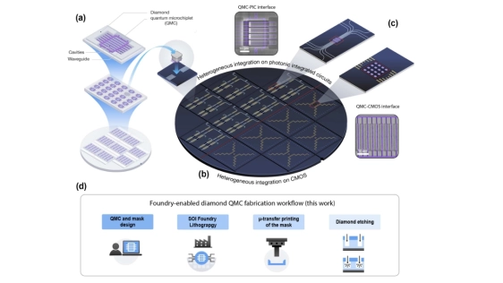
Quantum technologies promise secure communication networks and powerful new forms of information processing, but building these systems at scale remains a major challenge. Diamond is an especially attractive material for quantum devices because it can host atomic-scale defects that emit single photons and store quantum information with exceptional stability. However, fabricating the optical structures needed to control light in diamond typically relies on slow, bespoke processes that are difficult to scale. In this work, we introduce a manufacturing approach that brings diamond quantum photonics closer to industrial production. Instead of sequentially defining each device by lithography written directly on diamond, we fabricate high-precision silicon masks using commercial semiconductor foundries and transfer them onto diamond via microtransfer printing. These masks define large arrays of nanoscale optical structures, shifting the most demanding pattern-definition steps away from the diamond substrate, improving uniformity, yield, and throughput. Using this method, we demonstrate hundreds of diamond "quantum microchiplets" with improved optical performance and controlled interaction with quantum emitters. The chiplet format allows defective devices to be replaced and enables integration with existing photonic and electronic circuits. Our results show that high-quality diamond quantum devices can be produced using scalable, foundry-compatible techniques. This approach provides a practical pathway toward large-scale quantum photonic systems and hybrid quantum-classical technologies built on established semiconductor manufacturing infrastructure.
Keywords: Diamond quantum photonics, Foundry-compatible fabrication, Quantum microchiplets, Heterogeneous integration
To read the full article, click here
Related Chiplet
- Integrated voltage regulator (IVR) chiplet
- High-performance connectivity chiplets
- eFPGA Chiplet
- DPIQ Tx PICs
- IMDD Tx PICs
Related Technical Papers
- Cross Waveguide Design for Color-Centers in Diamond for Photonic Quantum Computing
- Codesign of quantum error-correcting codes and modular chiplets in the presence of defects
- Low-Loss Integration of High-Density Polymer Waveguides with Silicon Photonics for Co-Packaged Optics
- Quantum Dot DBR Lasers Monolithically Integrated on Silicon Photonics by In-Pocket Heteroepitaxy
Latest Technical Papers
- APEX: an Adaptive Photonic-Electronic Chiplet Interconnection Architecture for DNN Inference
- Formal Foundations for Known Good Reliable Die Screening in Chiplet-Based AI Systems-on-Chip
- Optimization of Test-Access Architectures and Test Scheduling for 2.5D/3D Integration
- Learning to Place Chiplets: A Multi-Objective Reinforcement Learning Approach
- ThAME: 3D Memory-Enabled Heterogeneous Accelerator for LLM Mixture of Experts