GPU-Accelerated Effective Resistance Analysis for 3D IC Power Delivery Network
By Jingchao Hu, Cheng Zhuo, Zhou Jin
College of Integrated Circuit, Zhejiang University
Abstract
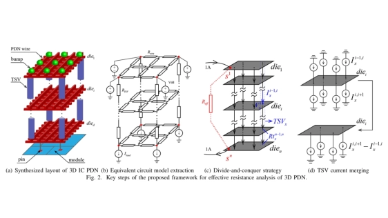
Three-dimensional (3D) integration is a critical technique for enhancing transistor density, improving power efficiency, and reducing interconnect delays. However, as current demands and design complexity increase, power deliver networks (PDNs) are facing growing challenges. Careful planning of through-silicon vias (TSVs) is essential for ensuring reliable PDNs, where effective resistance serves as a vital metric for the reliability. Ill-planned TSVs often cause 3D IC with unevenly distributed effective resistance and consequently severer IR Drop. In this paper, we propose a GPU-accelerated framework on accurate effective resistance analysis for early stage 3D IC PDNs. The proposed framework achieves a speedup of 5 to 6 orders of magnitude compared to the conventional direct solver, while maintaining negligible deviations in both maximum and average relative errors.
To read the full article, click here
Related Chiplet
- Optical Chiplet
- Reverse Gearbox Chiplet
- FlexGen Multi-Die Smart Network-on-Chip (NoC) IP
- Ncore Multi-Die Interconnect IP
- Integrated voltage regulator (IVR) chiplet
Related Technical Papers
- Co-Optimization of Power Delivery Network Design for 3-D Heterogeneous Integration of RRAM-Based Compute In-Memory Accelerators
- Toward Multi-kW Power Delivery Methodologies for Advanced 3D Heterogeneous Integration
- CUTh-Solver: GPU-Accelerated Sparse Matrix Solver for High-Resolution Thermal Simulation of 3D ICs
- ReVolt: Power Delivery Network-Aware Voltage Droop Control for 2.5D PIM Chiplet Architectures
Latest Technical Papers
- Beyond Host-Side Control: HBM Controller Partitioning Across Host and HBM Base Dies
- Chiplet-NAS: Chiplet-aware Neural Architecture Search for Efficient AI Inference on 2.5D Integration
- Scaling Up Analog CIM: A Simulation Framework for Topology-Aware Mapping
- AI-Based Image Enhancement Improves Detection of Interconnect Defects in Microelectronic Packaging
- Embodied Emissions of 2.5D and 3D Scaling in Chipletized GPUs for Low-Carbon AI