Enhancing Test Efficiency through Automated ATPG-Aware Lightweight Scan Instrumentation
By Sudipta Paria, Md Rezoan Ferdous, Aritra Dasgupta, Atri Chatterjee and Swarup Bhunia
Department of Electrical and Computer Engineering, University of Florida, Gainesville, FL, USA
Abstract
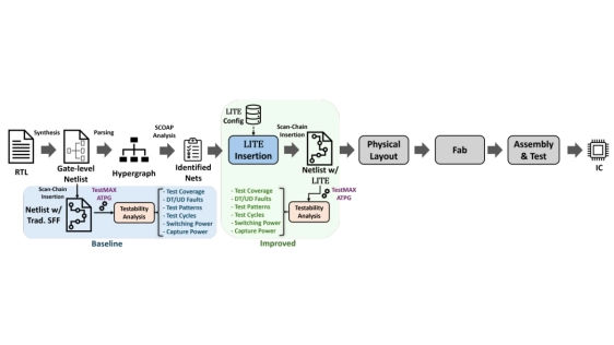
Scan-based Design-for-Testability (DFT) measures are prevalent in modern digital integrated circuits to achieve high test quality at low hardware cost. With the advent of 3D heterogeneous integration and chiplet-based systems, the role of scan is becoming ever more important due to its ability to make internal design nodes controllable and observable in a systematic and scalable manner. However, the effectiveness of scan-based DFT suffers from poor testability of internal nodes for complex circuits at deep logic levels. Existing solutions to address this problem primarily rely on Test Point Insertion (TPI) in the nodes with poor controllability or observability. However, TPI-based solutions, while an integral part of commercial practice, come at a high design and hardware cost. To address this issue, in this paper, we present LITE, a novel ATPG-aware lightweight scan instrumentation approach that utilizes the functional flip-flops in a scan chain to make multiple internal nodes observable and controllable in a low-cost, scalable manner. We provide both circuit-level design as well as an algorithmic approach for automating the insertion of LITE for design modifications. We show that LITE significantly improves the testability in terms of the number of patterns and test coverage for ATPG and random pattern testability, respectively, while incurring considerably lower overhead than TPI-based solutions.
Index Terms—Design-for-Testability (DFT), Scan Instrumentation, Testability, Observability, Controllability, Test Points, Fault Coverage, Automated Test Pattern Generation (ATPG).
To read the full article, click here
Related Chiplet
- Integrated voltage regulator (IVR) chiplet
- High-performance connectivity chiplets
- eFPGA Chiplet
- DPIQ Tx PICs
- IMDD Tx PICs
Related Technical Papers
- Complex Heterogeneous Integration Drives Innovation In Semiconductor Test
- Analysis Of Multi-Chiplet Package Designs And Requirements For Production Test Simplification
- 3D Stacked HBM and Compute Accelerators for LLM: Optimizing Thermal Management and Power Delivery Efficiency
- Hybrid surface pre-treatments for enhancing copper-to-copper direct bonding
Latest Technical Papers
- Thermo-mechanical reliability evaluation and comparative fatigue assessment of 2.5D chiplet packages with viscoelastic C4 underfill
- AI-Driven Thermal Mapping and Management in 3D Integrated Photonic Circuits
- CLIP-3D: Closed-Loop Evaluation of Performance and Physical Constraints for 3D ICs
- StreamDQ: Near-Memory Weight DeQuantization in Custom HBM for Scalable AI Inference Acceleration
- HCRMap: Pressure-Aware Hot-Expert Residency Mapping for 3.5D MoE Chiplet Inference