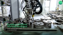
Sarcina Technology advances photonic package design to address key data center challenges 2025-06-04 11:06:00 Interconnects & Integration
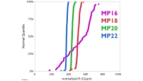
Imec demonstrates 16nm pitch Ru lines with record-low resistance obtained using a semi-damascene integration approach 2025-06-03 13:22:00 Standards & Research
Siemens expands OSAT Alliance membership to build domestic semiconductor supply chains 2025-05-30 08:27:00 Manufacturing & Supply Chain
AMD Acquires Enosemi to Accelerate Co-Packaged Optics Innovation for AI Systems 2025-05-29 08:16:00 Business & Deals
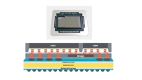
ASE Announces FOCoS-Bridge With TSV; Latest Package Technology Reduces Power Loss by 3x for Next-Generation AI and HPC Applications 2025-05-28 15:37:00 Manufacturing & Supply Chain
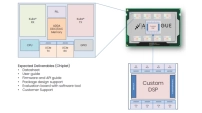
EdgeCortix Awarded New 3 Billion Yen NEDO Project to Develop Advanced Energy-Efficient AI Chiplet for Edge Inference and Learning 2025-05-28 07:47:00 Business & Deals
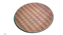
300mm RF silicon interposer platform for chiplet-based heterogeneous integration demonstrates record-low insertion loss at frequencies up to 325GHz 2025-05-27 12:17:00 Standards & Research
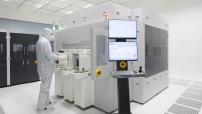
EV Group Brings Digital Lithography to Heterogeneous Integration HVM Applications with LITHOSCALE® XT 2025-05-26 12:44:00 Manufacturing & Supply Chain
Five workflows for tackling heterogeneous integration of chiplets for 2.5D/3D 2025-05-26 11:32:00 Analysis & Commentary
ITF World 2025: Imec’s Vision for Automotive Over the Long Haul 2025-05-25 17:13:00 Analysis & Commentary
Analogue Insight and Tetrivis Announce Joint Development of “Eurytion RFK1”, a UCIe based 12 nm Ka/Ku-Band RF Chiplet Transceiver 2025-05-23 03:51:00 Chiplets
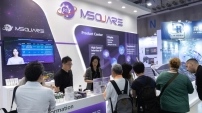
Powering AI with Chiplet Innovation: MSquare's ML100 IO Die Live at COMPUTEX 2025 2025-05-22 11:19:00 Other
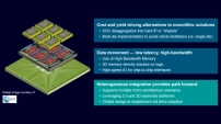
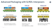
Advanced IC Packaging: The Roadmap to 3D IC Semiconductor Scaling 2025-05-20 16:19:00 Analysis & Commentary
Deca Announces Agreement with IBM to Bring High-Density Fan-Out Interposer Production to North America 2025-05-20 10:33:00 Manufacturing & Supply Chain
AEM Expands Access to Production-Proven SLT and Burn-In Ecosystem for Advanced Computing Customers 2025-05-20 07:41:00 Manufacturing & Supply Chain
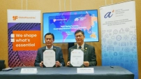
GlobalFoundries partners with A*STAR to accelerate advanced packaging innovation 2025-05-20 06:34:00 Ecosystem & Strategy