Advanced IC Packaging: The Roadmap to 3D IC Semiconductor Scaling
I recently had the privilege of sitting down with Jan Vardaman, President of TechSearch International and a leading authority in semiconductor packaging analysis, to discuss the transformative shifts occurring in integrated circuit design and manufacturing. “Our focus is entirely on advanced packaging, and the developments we’re seeing now are happening faster than ever,” Vardaman explained, setting the stage for an informative discussion about the semiconductor industry’s evolution toward chiplet-based architectures.
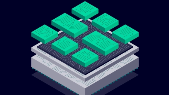
As the semiconductor industry approaches a projected market value of $1 trillion by 2030, the transition from traditional monolithic architectures to modular chiplet-based designs represents a fundamental shift in integrated circuit development. During our conversation, Vardaman provided crucial insights into why this transition is occurring: “The reason we’re seeing so much interest in the idea of the chiplet is that it offers a new way to design an IC. We can no longer afford to fabricate everything as a monolithic die on the most expensive nodes.”
To read the full article, click here
Related Chiplet
- Integrated voltage regulator (IVR) chiplet
- High-performance connectivity chiplets
- eFPGA Chiplet
- DPIQ Tx PICs
- IMDD Tx PICs
Related News
- IC-Link by imec joins TSMC 3DFabric® Alliance to accelerate advanced packaging and 3D IC innovation
- Siemens and Intel Foundry advance their collaboration to enable cutting-edge integrated circuits and advanced packaging solutions for 2D and 3D IC
- “From Lab to Fab” – Innovative front-end and advanced packaging technologies for the semiconductor value chain
- KLA Unveils Comprehensive IC Substrate Portfolio for a New Era of Advanced Semiconductor Packaging
Latest News
- Amkor Technology Announces Strategic Partnership with NVIDIA to Expand Advanced Packaging and Test for Next-Generation AI Infrastructure
- Synopsys Enables AMD Instinct™ MI455X GPU Design with Comprehensive Multi-Die Solution
- AI Data Centers Push Silicon Photonics Toward 300-mm Scale
- TYLsemi De-Risks Chiplets With New Business Model
- Cadence Introduces AuraStack AI Super Agent, the World’s First Agentic AI Platform for PCB and Advanced Packaging