Three-dimensional photonic integration for ultra-low-energy, high-bandwidth interchip data links
By Stuart Daudlin 1, Anthony Rizzo 1,2,3, Sunwoo Lee 4, Devesh Khilwani 4, Christine Ou 4, Songli Wang 1, Asher Novick 4, 1, Vignesh Gopal 1, Michael Cullen 1, Robert Parsons 1, Kaylx Jang 1, Alyosha Molnar 4 & Keren Bergman 1
1 Department of Electrical Engineering, Columbia University, New York, NY, USA.
2 Air Force Research Laboratory Information Directorate, Rome, NY, USA.
3 Thayer School of Engineering, Dartmouth College, Hanover, NH, USA. 4Department of Electrical and Computer Engineering, Cornell University, Ithaca, NY, USA.
Abstract
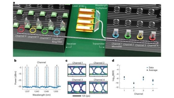
Artificial intelligence (AI) hardware is positioned to unlock revolutionary computational abilities by leveraging vast distributed networks of advanced semiconductor chips. However, a barrier for AI scaling is the disproportionately high energy and chip area required to transmit data between the chips. Here we present a solution to this long-standing overhead through dense three-dimensional (3D) integration of photonics and electronics. With 80 photonic transmitters and receivers occupying a combined chip footprint of only 0.3 mm2, our platform achieves an order-of-magnitude-greater number of 3D-integrated channels than prior demonstrations. This enables both high-bandwidth (800 Gb s−1) and highly efficient, dense (5.3 Tb s−1 mm−2) 3D channels. The transceiver energy efficiency is showcased by a state-of-the-art 50 fJ and 70 fJ per communicated bit from the transmitter and receiver front ends, respectively, operating at 10 Gb s−1per channel. Furthermore, the design is compatible with commercial complementary metal–oxide–semiconductor foundries fabrication on 300-mm-sized wafers, providing a route to mass production. Such ultra-energy-efficient, high-bandwidth data communication links promise to eliminate the bandwidth bottleneck between spatially distinct compute nodes and support the scaling of future AI computing hardware.
To read the full article, click here
Related Chiplet
- Integrated voltage regulator (IVR) chiplet
- High-performance connectivity chiplets
- eFPGA Chiplet
- DPIQ Tx PICs
- IMDD Tx PICs
Related Technical Papers
- Low-Loss Integration of High-Density Polymer Waveguides with Silicon Photonics for Co-Packaged Optics
- Advanced Optical Integration Processes for Photonic-Integrated Circuit Packaging
- Heterogeneous Integration - Chiplets
- Why package lithography matters in heterogeneous chiplet integration
Latest Technical Papers
- APEX: an Adaptive Photonic-Electronic Chiplet Interconnection Architecture for DNN Inference
- Formal Foundations for Known Good Reliable Die Screening in Chiplet-Based AI Systems-on-Chip
- Optimization of Test-Access Architectures and Test Scheduling for 2.5D/3D Integration
- Learning to Place Chiplets: A Multi-Objective Reinforcement Learning Approach
- ThAME: 3D Memory-Enabled Heterogeneous Accelerator for LLM Mixture of Experts