Thermal Tuning Overhead in Wafer-Scale Optical Interconnects for LLM MoE Training: A Cross-Layer Analysis and Ferroelectric-Based Mitigation
By Seongwon Yoon, Pin-Jun Chen, Shimeng Yu
Georgia Institute of Technology, USA
Abstract
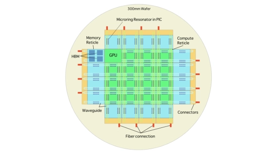
The rapid scaling of large language models (LLMs), particularly mixture-of-experts (MoE) architectures, has intensified interconnect demands because expert-parallel execution is communication-intensive. Wafer-scale optical interconnects based on dense wavelength-division multiplexing (DWDM) offer a promising path to higher bandwidth; however, conventional microring-resonator (MRR)-based links rely on thermo-optic tuning and are therefore vulnerable to workload-induced thermal fluctuations. In this work, we present a cross-layer analysis of wafer-scale optical interconnects for MoE workloads that combines workload profiling, packet-level network simulation, and transient thermal analysis. We implement a wafer-scale topology in the ht-sim simulator and construct an Ansys thermal model of a 3D-integrated GPU/EIC/PIC stack. Our results show that transient temperature variations can exceed the tracking capability of conventional thermo-optic control loops and thereby introduce repeated tuning stalls during communication phases. The stall durations injected into the network simulation are derived directly from the thermal model rather than assumed. We further evaluate a ferroelectric-based electro-optic tuning mechanism that removes the continuous thermal-tuning requirement. In a four-layer proxy simulation across three MoE models, eliminating the tuning stalls yields speedups of 2.7x for Mixtral 8x7B, 3.8x for Qwen-MoE 14.3B, and 3.3x for LLaMA-MoE 6.7B relative to the thermo-optic case. These results indicate that minimizing photonic tuning latency is important for realizing the performance potential of optical interconnects in large-scale AI systems.
CCS Concepts: • Hardware → Emerging optical and photonic technologies; Interconnection networks; • Computing methodologies → Distributed computing methodologies.
Additional Key Words and Phrases: mixture-of-experts, silicon photonics, optical interconnects, wafer-scale systems, photonic interposer
To read the full article, click here
Related Chiplet
- FlexGen Multi-Die Smart Network-on-Chip (NoC) IP
- Ncore Multi-Die Interconnect IP
- Integrated voltage regulator (IVR) chiplet
- High-performance connectivity chiplets
- eFPGA Chiplet
Related Technical Papers
- ChipLight: Cross-Layer Optimization of Chiplet Design with Optical Interconnects for LLM Training
- Predictive Software Scheduling as an Early-Warning Hint Layer for Optical Engine Thermal Drift in Heterogeneous SoIC Packaging
- 3D Stacked HBM and Compute Accelerators for LLM: Optimizing Thermal Management and Power Delivery Efficiency
- DeepOHeat-v1: Efficient Operator Learning for Fast and Trustworthy Thermal Simulation and Optimization in 3D-IC Design
Latest Technical Papers
- Divide and conquer: Scalable performance and energy in MCM GPUs
- A Composable AI-Accelerated Iterative Solver for 3D-IC Thermal Modeling
- QBX: A Compiler for 2-local Qubit Hamiltonian Simulation on Quantum Chiplets
- U-Can-Inject-Errors (UCIe): A Protocol-Aware Hardware Trojan for FPGA Chiplet Links
- The Power of Indirection: Scaling Switches Beyond Silicon Boundaries