Plasma Etch Process Optimization for Photonic-Grade Diamond-on-Insulator Substrates and Thickness Evaluation using Colorimetry
By Tianyin Chen, Alessio Mirandaa, Leyla Ramia, Ryoichi Ishiharaa, Salahuddin Nur
Delft University of Technology, The Netherlands
Abstract
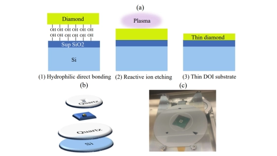
Diamond color-center qubits integrated with photonic circuits can be initialized, manipulated, entangled, and read individually with high fidelity, making them attractive for large-scale modular quantum computers, quantum networks, and distributed quantum sensing. However, the limited size of heteroepitaxially grown single-crystal diamond (SCD) and photonic-grade diamond-on-insulator (DOI) substrates remains a challenge for integration with existing manufacturing processes. Here, we develop a plasma etch recipe to thin direct-bonded (100) SCD membranes (<50 µm) into large-area, thin-film DOI substrates, and demonstrate free-standing photonic chiplets fabricated from the resulting DOI. The ICP-RIE recipe preserves diamond bonding, provides sufficient micromasking and surface-quality control, and enables thin-film DOI manufacture. We thin a 10 µm diamond plate bonded to SiO₂/Si and obtain a photonic-grade DOI substrate with diamond thickness ≤300 nm. The DOI film is around 300 nm thick over 0.5 x 0.5 mm², with surface roughness < 0.5 nm, while the bonding interface remains intact. Diamond photonic chiplets are fabricated on this DOI substrate using a standard two-step lithography process, without complex thin-film transfer, under-etching, or pedestal formation. We also present a colorimetric study of diamond visibility on SiO₂ and quantify color differences across thicknesses in common colorimetric spaces. This analysis enables automatic diamond-thickness extrapolation from standard optical microscope images with 5 nm resolution, in good agreement with white-light interferometry (WLI) measurements. The DOI substrate and colorimetric thickness-evaluation method provide an effective fabrication platform and reliable validation route for scalable manufacturing of diamond nanophotonic devices, opening a path toward large-scale integrated quantum systems.
To read the full article, click here
Related Chiplet
- Integrated voltage regulator (IVR) chiplet
- High-performance connectivity chiplets
- eFPGA Chiplet
- DPIQ Tx PICs
- IMDD Tx PICs
Related Technical Papers
- Wafer Warpage of Silicon Interposer in Manufacturing Processes for High Density 2.5D Advanced Packaging: Causes, Measurement, Analysis and Optimization
- FoldedHexaTorus: An Inter-Chiplet Interconnect Topology for Chiplet-based Systems using Organic and Glass Substrates
- ATSim: A Fast and Accurate Simulation Framework for 2.5D/3D Chiplet Thermal Design Optimization
- DeepOHeat-v1: Efficient Operator Learning for Fast and Trustworthy Thermal Simulation and Optimization in 3D-IC Design
Latest Technical Papers
- StreamDQ: Near-Memory Weight DeQuantization in Custom HBM for Scalable AI Inference Acceleration
- HCRMap: Pressure-Aware Hot-Expert Residency Mapping for 3.5D MoE Chiplet Inference
- Chiplet3D: Pin- and Thermal-Aware 3D Chiplet Floorplanning via Convolution-Embedded MILP
- The Signal-Integrity Control Strategy of a TSV Array for a Chiplet-Based System
- ThermoDSE: A Thermal-Aware and Comprehensive Design Space Exploration for Chiplet-Based DNN Accelerators