Escaping Flatland: A Placement Flow for Enabling 3D FPGAs
By Cong Hao 1, Andrew B. Kahng 2, Bodhisatta Pramanik 2, Ismael Youssef 1
1 Georgia Tech, Atlanta, GA, USA
2 UCSan Diego, San Diego, CA, USA
Abstract
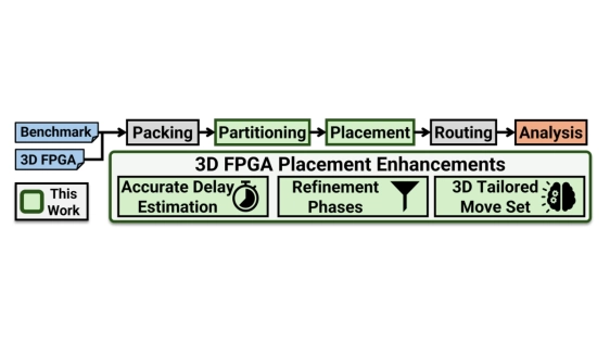
3D field-programmable gate arrays (FPGAs) promise higher performance through vertical integration. However, existing placement tools, largely inherited from 2D frameworks, fail to capture the unique delay characteristics and optimization dynamics of 3D fabrics. We introduce a 3D FPGA placement flow that integrates partitioning-based initialization, adaptive cost scheduling, refined delay estimation, and a simulated annealing move set -- all targeted at 3D FPGA architecture. Together, these enhancements improve timing estimates and the exploration of layer assignments during placement. Compared to Verilog-To-Routing (VTR), our experiments show geometric-mean (max) critical-path delay reductions of ~3% (~7%), ~2% (~4%), ~3% (~8%), and ~6% (~18%) for four 3D architectures: 3D CB, 3D CB-O, 3D CB-I, and 3D SB, respectively. We also achieve geometric-mean (max) routed wirelength reductions of ~1% (~3%), ~2% (~8%), < 1% (~5%), and ~5% (~10%), respectively. Our work will be permissively open-sourced on GitHub.
To read the full article, click here
Related Chiplet
- Integrated voltage regulator (IVR) chiplet
- High-performance connectivity chiplets
- eFPGA Chiplet
- DPIQ Tx PICs
- IMDD Tx PICs
Related Technical Papers
- 3D Electronic-Photonic Heterogenous Interconnect Platforms Enabling Energy-Efficient Scalable Architectures For Future HPC Systems
- DTCO of NOR-Type IGZO FeFETs for 3D Heterogeneous AI Memories: A Read-Centric Perspective
- 3DLS: A 3D Logic-Stacked Architecture for Disaggregated LLM Serving
- 3D Stacked HBM and Compute Accelerators for LLM: Optimizing Thermal Management and Power Delivery Efficiency
Latest Technical Papers
- APEX: an Adaptive Photonic-Electronic Chiplet Interconnection Architecture for DNN Inference
- Formal Foundations for Known Good Reliable Die Screening in Chiplet-Based AI Systems-on-Chip
- Optimization of Test-Access Architectures and Test Scheduling for 2.5D/3D Integration
- Learning to Place Chiplets: A Multi-Objective Reinforcement Learning Approach
- ThAME: 3D Memory-Enabled Heterogeneous Accelerator for LLM Mixture of Experts