Cross Waveguide Design for Color-Centers in Diamond for Photonic Quantum Computing
By Alessio Miranda 1,2, Ryoichi Ishihara 1,2 and Salahuddin Nur 1
1 Department of Quantum Computer Engineering, Faculty of Electrical Engineering Mathematics and Computer Science, Delft University of Technology, Delft, The Netherlands
2 QuTech, Delft University of Technology, Delft, The Netherlands
Abstract
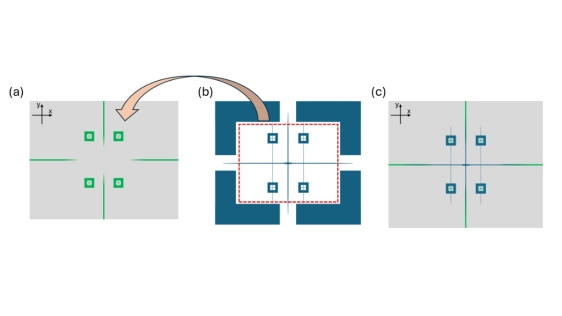
Color centers in diamond are a promising platform for quantum computing applications because of their optical and spin properties. However, diamond presents some technological challenges that limit its use in complex or large photonic circuits. To mitigate these limitations, it is technically effective to separate the smallest possible diamond photonic structures or chiplet containing the color center(s) from the rest of the circuit, which is fabricated on another material platform, and then heterogeneously integrate them. Considering efficient excitation and photon collection from waveguide-coupled color centers, we design a cross waveguide as the primary component of our chiplet to access the color centers, channeling excitation and emitted photons into different waveguides, and connecting the structure to the other components of the photonic circuit. The chiplet containing the cross waveguide and supporting structures requires careful optimization of each subcomponent. The receptor's design is also critical for optimal signal transmission. In this paper, we develop a simple but efficient methodology to optimize the main components constituting both the chiplet and the receptor for their synergistic operation. The designed structure has an excitation-to-emission conversion of more than 5.4%, crosstalk of less than -40 dB, a working bandwidth of 160 nm, fabrication feasibility and tolerance within the limits of modern nanofabrication, and a mechanical solid structure with a footprint of less than 2000 µm².
To read the full article, click here
Related Chiplet
- Integrated voltage regulator (IVR) chiplet
- High-performance connectivity chiplets
- eFPGA Chiplet
- DPIQ Tx PICs
- IMDD Tx PICs
Related Technical Papers
- Advances in waveguide to waveguide couplers for 3D integrated photonic packaging
- A Comprehensive Design Framework for Vertical Power Delivery in High-Performance Computing
- PICNIC: Silicon Photonic Interconnected Chiplets with Computational Network and In-memory Computing for LLM Inference Acceleration
- Foundry-Enabled Patterning of Diamond Quantum Microchiplets for Scalable Quantum Photonics
Latest Technical Papers
- AI-Driven Thermal Mapping and Management in 3D Integrated Photonic Circuits
- CLIP-3D: Closed-Loop Evaluation of Performance and Physical Constraints for 3D ICs
- StreamDQ: Near-Memory Weight DeQuantization in Custom HBM for Scalable AI Inference Acceleration
- HCRMap: Pressure-Aware Hot-Expert Residency Mapping for 3.5D MoE Chiplet Inference
- Chiplet3D: Pin- and Thermal-Aware 3D Chiplet Floorplanning via Convolution-Embedded MILP