3D optoelectronics and co-packaged optics: when solving the wrong problems stalls deployment
By Yasha Yi 1,2 and Danny Wilkerson 3
1 Intelligent Optoelectronics Laboratory and Connected Systems Institute, University of Wisconsin, Milwaukee
2 Microsystems Technology Laboratory, Massachusetts Institute of Technology, Cambridge
3 Invictus Innovation EV Technology
Abstract
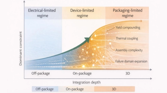
The rapid growth of AI and accelerator-driven workloads is forcing a fundamental rethinking of optical interconnect architectures in datacenters. Co-packaged optics and three-dimensional photonic integration have emerged as promising solutions to overcome the energy and bandwidth limitations of electrical I/O. Yet, as optics move closer to compute, packaging, thermal management, and system-level robustness increasingly dominate performance and scalability. Here, we argue that co-packaged optics should not be viewed as a component-level optimization, but as an architectural commitment that reshapes the boundaries between photonics, electronics, and system design. We examine how heterogeneous integration strategies, chiplet-based optics, and emerging packaging platforms redefine scaling laws for AI systems, often introducing trade-offs that are underappreciated in device-centric analyses. Looking forward, we discuss why standardization, serviceability, and thermal-aware co-design will be decisive in determining whether co-packaged optics can transition from early deployment to widespread adoption in AI-scale datacenters.
To read the full article, click here
Related Chiplet
- eFPGA Chiplet
- DPIQ Tx PICs
- IMDD Tx PICs
- Near-Packaged Optics (NPO) Chiplet Solution
- High Performance Droplet
Related Technical Papers
- TA3D: Timing-Aware 3D IC Partitioning and Placement by Optimizing the Critical Path
- CHICO-Agent: An LLM Agent for the Cross-layer Optimization of 2.5D and 3D Chiplet-based Systems
- The Next Frontier in Semiconductor Innovation: Chiplets and the Rise of 3D-ICs
- MFIT : Multi-FIdelity Thermal Modeling for 2.5D and 3D Multi-Chiplet Architectures
Latest Technical Papers
- The Signal-Integrity Control Strategy of a TSV Array for a Chiplet-Based System
- ThermoDSE: A Thermal-Aware and Comprehensive Design Space Exploration for Chiplet-Based DNN Accelerators
- GPU-Accelerated Effective Resistance Analysis for 3D IC Power Delivery Network
- FAPlace: Joint Optimization of Chiplet Placement and Interposer Footprint for 2.5D Systems
- Chiplet-Escape: An Efficient Obstacle-Avoiding Escape Routing Method for Die-to-Die Interconnections in Chiplet-Based Designs