Spying Across Chiplets: Side-Channel Attacks in 2.5/3D Integrated Systems
By Giorgio Di Natale 1, Christelle Rabache 1, Pierre-Louis Hellier 1, Florence Podevin 1, Sylvain Bourdel 1, Romain Siragusa 2, Paolo Maistri 1
1 Univ. Grenoble Alpes, CNRS, Grenoble INP, TIMA, Grenoble, France
2 Univ. Grenoble Alpes, Grenoble INP, LCIS, Valence, France
Abstract
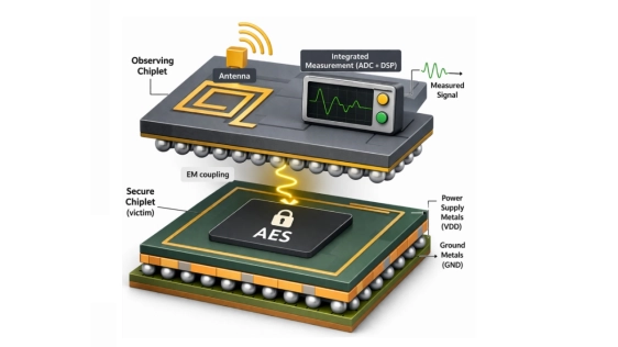
Advanced packaging and chiplet-based integration are increasingly adopted to build complex heterogeneous systems beyond the limits of monolithic scaling. While these architectures offer major benefits in terms of modularity, yield, and performance, they also introduce new physical attack surfaces. In this paper, we show that side-channel attacks can be mounted across chiplets within the same package or stack. Our key idea is that a communication-oriented chiplet, originally intended to interact with the external environment through an antenna, an RFID-like element, or another contactless coupling structure, can be repurposed as an internal observation platform. We formalize this threat through a realistic adversary model, describe the corresponding attack principle, and experimentally assess its feasibility. The obtained results demonstrate that signals captured through such a communication-oriented interface can reveal information correlated with the activity of a neighboring victim chiplet.
To read the full article, click here
Related Chiplet
- Integrated voltage regulator (IVR) chiplet
- High-performance connectivity chiplets
- eFPGA Chiplet
- DPIQ Tx PICs
- IMDD Tx PICs
Related Technical Papers
- Resister: A Resilient Interposer Architecture for Chiplet to Mitigate Timing Side-Channel Attacks
- What’s Next for Multi-Die Systems in 2024?
- The Next Frontier in Semiconductor Innovation: Chiplets and the Rise of 3D-ICs
- Codesign of quantum error-correcting codes and modular chiplets in the presence of defects
Latest Technical Papers
- ThAME: 3D Memory-Enabled Heterogeneous Accelerator for LLM Mixture of Experts
- Thermo-mechanical reliability evaluation and comparative fatigue assessment of 2.5D chiplet packages with viscoelastic C4 underfill
- AI-Driven Thermal Mapping and Management in 3D Integrated Photonic Circuits
- CLIP-3D: Closed-Loop Evaluation of Performance and Physical Constraints for 3D ICs
- StreamDQ: Near-Memory Weight DeQuantization in Custom HBM for Scalable AI Inference Acceleration