How to Streamline Your Advanced Package (Chiplet, 3DIC) Interconnect Designs

Key takeaways:
- Advanced package (Chiplet 3DIC) interconnect designs introduce significant technical challenges for engineers and other stakeholders.
- Existing electronic design automation (EDA) solutions lack the speed, capacity or accuracy required for the advanced package (Chiplet, 3DIC) interconnect designs and overcoming signal integrity issues.
- 3D Interconnect design, optimization, and verification tools from Keysight bridge this crucial design gap, enabling engineers to design chiplets more efficiently and effectively for emerging and evolving markets like artificial intelligence and data centers.
Monolithic system-on-chip (SoC) designs was once a popular choice; however they face significant constraints in the era of AI. By forcing all chip functions into a single die and process node, they reduce engineering, manufacturing, and design cost flexibility.
In contrast, the multi-die nature of chiplets enables different SoC functions to be designed and verified independently and fabricated on a cost-effective process node.
This blog post explains how Keysight’s Chiplet PHY Designer, Chiplet 3D Interconnect Designer, and 3D Interconnect Designer address early-stage uncertainties in the advanced package (Chiplet, 3DIC) interconnect designs with high-fidelity modeling, simulation solutions, and workflow automation.
What are the market drivers behind chiplets?
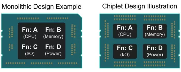
Figure 1. Monolithic versus chiplet-based chip designs
Compared to monolithic SoCs, chiplet-based SoCs confer several benefits:
- better energy efficiency and lower power consumption,eg. pJ/bit
- more cost-effective using mix-and-match process node
- better thermal performance
- higher fabrication yields
- heterogeneous multi-vendor integration through open standards like the universal chiplet interconnect express (UCIe) and bunch of wires (BoW)
- faster development time
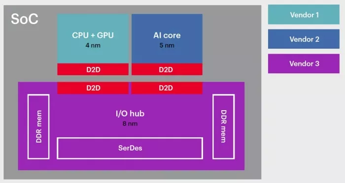
Figure 2. A multi-die chiplets from different vendors
As a result, the chiplet ecosystem is rapidly expanding in crucial domains like:
- artificial intelligence (AI)
- high-performance computing (HPC)
- data centers
- networking (gigabit and optical)
- automotive
- radio frequency applications (like 5G and 6G)
At the same time, the complexity of chiplet connectivity is also scaling quickly, starting from 2D, and 2.5D3D stacked advanced packages. These packaging technologies rely on silicon interposers, silicon bridges, and organic substrates that create various design challenges and associated product-to-market risks.
What are the late-stage signal integrity risks of chiplet interconnects?
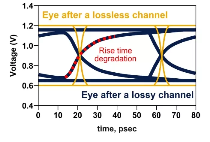
Figure 3. Eye diagrams of a lossy channel (black) and a lossless channel (yellow), with rise time degradation shown by the red dotted line.
The unique characteristics of chiplets and the advanced packaging create significant concerns for signal integrity (SI) and power integrity (PI) engineers, for example, unconventional ground return path using hatched ground planes instead solid ground planes.
Late-stage discovery of SI/PI issues can be catastrophic, leading to costly design respins. Early-stage prevention is ideal, but unfortunately, existing EDA workflows often lack the tools to do so effectively.
Key concerns are outlined below:
- Ground/return path risks: Hatched (waffled) ground planes in the silicon bridges and interposers can disrupt signal return paths. Unfortunately, they are necessary due to silicon manufacturing constraints; however, they are very difficult to model If not modeled correctly, they can lead to SI failures, such as closed eye, compliance issues, and non-optimum performance.
- Crosstalk: As interconnects become denser (e.g., in 2.5D and 3D stacking) and with the increased use of hatched ground planes, crosstalk could increase.
- Reflections go up due to impedance mismatches due to non-uniform hatched ground planes.
- Strict standards: Interconnect standards like UCIe and BoW have rigorous electrical requirements to ensure interoperability. SI engineers adhere to 1) correct voltage transfer functions (VTF) to ensure that insertion loss and crosstalk meet the requirements for given data rates and packaging types, 2) eye margin standards at the receivers to enable error-free transmissions, and 3) well-behaved forwarded clocking including QDR.
- Probing difficulties: It’s nearly impossible to physically probe these dense interconnects with very small pitch size at the u-bump level. Engineers must rely entirely on simulations and virtual probes.
- Heterogeneous integration risks: Since chiplets often come from multiple vendors, interoperability becomes complicated. Engineers must verify that the cumulative effects of different materials, process nodes, and signaling protocols work seamlessly . Ensuring stable power delivery across chiplets without voltage drops or resonances is critical.
What concerns high-speed digital designers about chiplet interconnects?
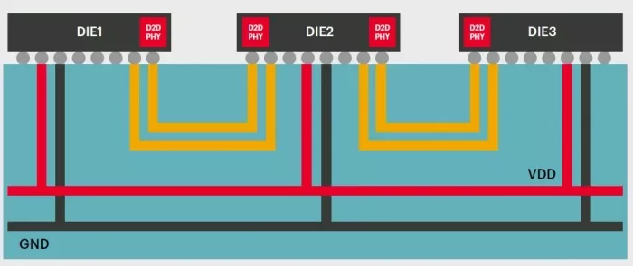
Figure 4. Simplified chiplet package view with die-to-die PHY interfaces (orange traces)
Apart from the SI concerns above, high-speed digital design engineers also worry over the following aspects of chiplet interconnects:
- Package modeling difficulties: Accurate modeling is lacking for stacked interconnects, high-speed digital wide buses with hatched grounds (such as UCIe 2.5D/3D packages), Through silicon vias (TSVs), and hybrid bonding. These approaches are used in high-bandwidth memory and graphical processing units (GPUs), which are critical to AI data centers.
- Higher loss in Silicon: High-speed interconnects attenuate high-frequency components more than low-frequency ones, leading to rise-time degradation and intersymbol interference (ISI). The resulting slopes and closure in the eye diagram reduce the timing and voltage margins for reliable transmission. This can be amplified in lossy silicon materials.
- Die-to-die (D2D) communication testing: Standardized interfaces between chiplets from different vendors are difficult. Engineers must verify interoperability without being able to probe inside the finished package. Virtual prototyping and simulations are the only viable verification methods.
What worries architects and managers about chiplet interconnect designs?
The early-stage blind spots in chiplet interconnect decisions worry various other stakeholders in the semiconductor industry. Modern multi-die systems have to decide a good system partitioning, choose the right package technology , for example silicon or organic interposers, and silicon bridges. These decisions must be made much before the package layout stage, when there are many unknowns and risk is highest.
Apart from engineers, these concerns are shared by:
- system architects who evaluate key decisions
- engineering managers who are accountable for the schedule and risks
- technical executives responsible for platform decisions
- procurement teams evaluating EDA solutions
Other concerns include:
- Optimizing the package stack-ups
- Vertical power delivery for low voltage and high current applications
- pushing the SI constraints of high-speed D2D standards earlier up the design flow, and the risks of costly respins due to late discovery of SI issues
- lack of fast, accurate modeling, optimization, and validation solutions for productive design space exploration in the early phases, before the layout stage
- lack of advanced package modeling for chiplets and three-dimensional integrated circuits (3DICs)
- workflow and tool fragmentation between the architecture, layout, and SI teams
- reducing system design cycles by maintaining accuracy from schematic to tape-off
What are the limitations of traditional verification?
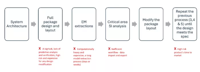
Figure 5. Traditional design workflow
Traditional linear EDA workflows fail to address the above concerns of engineers and other stakeholders because of two deficiencies:
- High risk and computationally heavy post layout driven workflow
- Lack of design optimization and verification before a full package layout
Traditional post-layout driven workflow makes the design optimization and verification process hard since it requires a very tedious workflow and computationally resource heavy EM extractions. Especially the challenges are amplified in the application of advanced package designs where silicon interposers and bridges are used with hatched grounds. They struggle to calculate the complex physics of hatched ground patterns.
However, most circuit level pre-layout methods also lack the high-fidelity modeling accuracy required to predict high-speed D2D link margins and compliance with UCIe or BoW standards early in the design cycle.
Additionally, these traditional EDA tools do not seamlessly integrate interconnects with PHY-level compliance verification, forcing teams into manual, error-prone data integration.
Meanwhile, post-layout EM workflow lacks the required capabilities to bridge this gap. They are too slow and resource-heavy to be useful for rapid early-stage design exploration.
Why are Keysight's 3D interconnect design solution better?
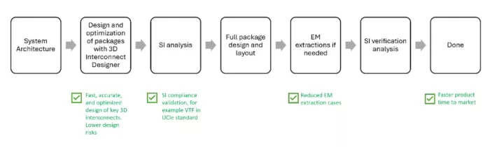
Figure 6. Practical and efficient advanced package design workflow using Keysight EDA
Keysight addresses these limitations through next-generation design solutions for 3D interconnects in advanced packages . These solutions include:
- Chiplet PHY Designer
- Chiplet 3D Interconnect Designer
- 3D Interconnect Designer
These solutions enable rapid design space exploration with fast, accurate insights based on physical designs without requiring a full package layout.
They deliver the following benefits:
- Enable complete wide bus design and analysis with less computational resources
- Effectively handle the modeling of signal transmission with hatched grounds
- Reduce re-spins by enabling complex design space explorations early in the design process.
- Comply with compliance specifications like VTF and eye margin imposed by the UCIe standard from the earliest design stages.
- Cut down the product’s time-to-market for chiplet D2D interconnects.
- Concurrently optimize cost, performance, power, and signal reliability through automated sweeping of design variables (like termination resistance).
- Provide automated and AI-ready workflows.
Chiplet PHY Designer
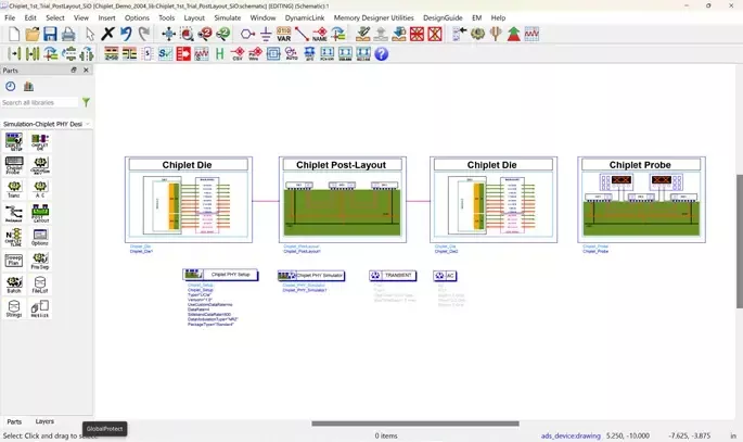
Figure 7. Chiplet system simulation with the Keysight Chiplet PHY Designer
Keysight's Chiplet PHY Designer is the leading physical layer EDA solution for the chiplet standards, UCIe and BoW, for link margin and compliance analysis.
Chiplet PHY Designer capabilities include:
- Support Chiplet standards, UCIe and BoW
- Support UCIe-S, UCIe-S, and UCIe-3D specifications
- die-to-die link performance analysis, eye-diagram and BER, as per system-level requirements
- integrated die-to-die physical interface design through the Chiplet 3D Interconnect Designer
- support for advanced package designs with silicon bridges and interposers Compliance measure, VTF
- Various clocking support double data rate (DDR), and quad data rate clock (QDR)
Chiplet 3D Interconnect Designer
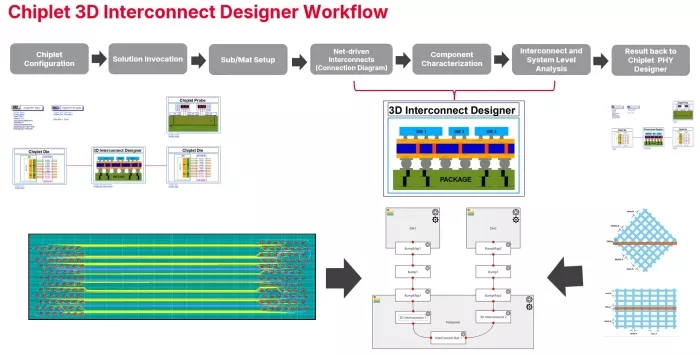
Figure 8. Chiplet 3D Interconnect Designer modeling
Keysight's Chiplet 3D Interconnect Designer is 3D Interconnect Designer version integrated into ADS Chiplet PHY Designer. It starts the workflow from Chiplet PHY Designer and completes the advanced package design with the knowledge of Chiplet standards, UCIe and BoW. Designers can design chiplet die-to-die interconnects on silicon bridges and interposers. The designed advanced package with automated net-name assignment can be dropped directly into the Chiplet PHY Designer for link margin analysis and compliance measurements.
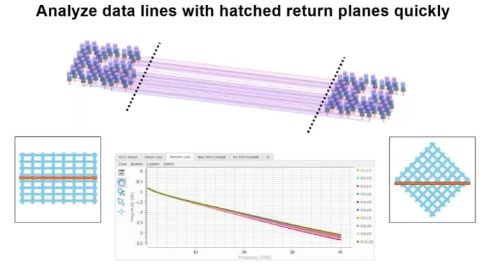
Figure 9. Hatched ground plane analysis
It supports complex hatched/waffled ground plane structures. Engineers can identify and resolve grounding and crosstalk issues from the early design stages before committing to a full-scale package layout for wide-bus systems.
Other key capabilities include:
- Standard-driven bump maps for UCIe and BoW
- Fast and accurate physical channel modeling
- Rectangular/Diamond style hatched grounds
- Via designs with breakout feed lines – straight and serpentine breakout lines
- Automated net name assignment
- Automated wire connection through connection diagram
- Stack-up design with import and export capability
- Component- and interconnect- level analysis
- Swept variable design analysis
- Guided user-friendly workflow
3D Interconnect Designer
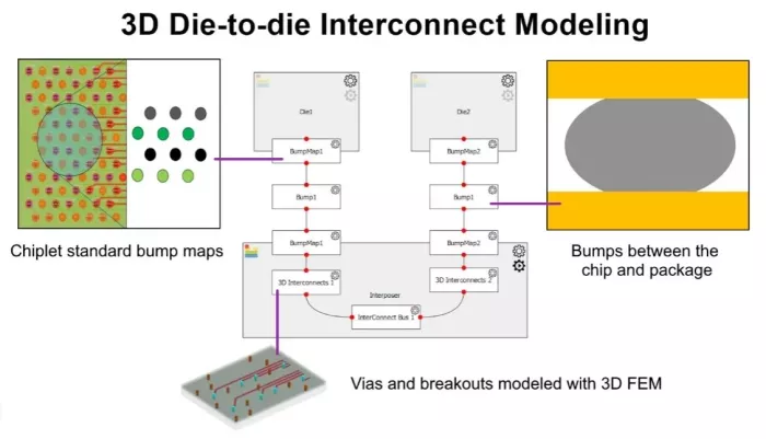
Figure 10. 3D Interconnect Designer
The 3D Interconnect Designer is a new standalone and universal solution to design any kind of interconnect, including chiplets, 3DICs, packages, and printed circuit boards. This version doesn’t require ADS and Chiplet PHY Designer and can work with other EDA workflows
Key capabilities include:
- Inclusive of Chiplet 3D Interconnect Designer
- Support multi-die, stacked-die, complex 3D packages
- Model complete 3D interconnects from PCB to micro bumps throught laminates and interposers
- Support fast, accurate physical channel modeling with vias, micro bumps, transmission lines, and solder balls
- Support for hatched/waffled grounds
- Support for stacked die and 3DIC architecture
- Works standalone with all popular EDA environments, including Keysight ADS
How do Keysight tools facilitate chiplet interconnect design?
The UCIe specification demands stringent and comprehensive requirements. Keysight EDA tools enable automated compliance testing against these strict requirements, including VTF, eye mask tests, low latency, and forwarded clocking for DDR and QDR. The tools automatically calculate metrics like VTF loss and crosstalk and generate actionable reports.
BoW is more flexible and lacks the direct electrical requirements for loss and crosstalk. To enable comparisons and trade-offs of UCIe and BoW designs, Keysight’s tools enable evaluation of BoW designs using the same consistent standard-driven metrics as UCIe.
Silicon versus organic evaluation
Silicon interposers are essential for high-performance applications. They support ultra-dense wiring for high bandwidths and allow connections with very tight pitches. However, they’re expensive, size-limited by semiconductor fabrication reticle limits, and prone to thermal warping issues. Hatched ground planes prevent warping but introduce potential SI issues.
Organic substrates are more cost-effective and larger, but struggle to support the high-density signal requirements of chiplet interconnects for AI or HPC.
The Chiplet 3D Interconnect Designer facilitates evaluation and selection of silicon versus organics. It’s designed for fast, accurate modeling of the complex physics of hatched ground planes. Physically-aware pre-layout simulations enable the crucial shift-left strategy. Engineers can identify SI/PI bottlenecks of interposer geometry, like impedance discontinuities and return path issues, from early on.
Engineers can simulate both silicon and organic interposer configurations before drawing the final layout. They can evaluate, early in the design flow, whether an organic substrate will meet the requirements of a design that would otherwise require a silicon interposer.
Routing feasibility
These Keysight tools enable the evaluation of routing feasibility in high-speed digital and chiplet-based designs. They allow engineers to analyze, optimize, and validate routing before fabrication.
Through physically-aware pre-layout exploration, designers can analyze channel links and routing architectures early in the design cycle to identify and mitigate SI/PI issues. Designers can compare different routing configurations.
The tools provide smart connection wizards and automated routing and breakout features (like auto-routing for vias) to reduce manual setup time and minimize human error.
They provide immediate feedback on how layout changes — adding return vias or changing spacing — affect SI/PI, enabling engineers to quickly iterate on routing strategies until they meet performance targets.
Ground structure impacts
Keysight tools enable accurate prediction and analysis of hatched ground planes used in advanced packaging.
The Chiplet 3D Interconnect Designer is explicitly designed to model these complex geometries and their impacts on SI.
The 3D Interconnect Designer provides the same capability for broader 3DIC and package designs. Complex ground structures can be modeled correctly in any EDA environment.
Choose Keysight for your chiplet interconnect designs
This blog post explored chiplet interconnect concerns and how Keysight's solutions address them.
With Keysight Chiplet PHY Designer, Chiplet 3D Interconnect Designer, and 3D Interconnect Designer, you can reduce your risks, accelerate your time to market, and improve your design confidence.
Contact us for demos and recommendations on chiplet interconnect designs.
Related Chiplet
- eFPGA Chiplet
- DPIQ Tx PICs
- IMDD Tx PICs
- Near-Packaged Optics (NPO) Chiplet Solution
- High Performance Droplet
Related Blogs
- Bring Your Own RTL to Zero ASIC's Chiplet Ecosystem
- GUC Leverages 3DIC Compiler to Enable 2.5D/3D Multi-Die Package
- UMI: Extending Chiplet Interconnect Standards To Deal With The Memory Wall
- Case Study: How to Sign Off Your UCIe Interface
Latest Blogs
- How Intel Foundry Packaging Technologies Redefine AI and HPC Scalability Limits at ECTC 2026
- From complexity to simplicity: Scaling and future-proofing chiplets with AMBA®︎ CHI C2C property negotiation
- High-Speed Heterogeneous Integration with Multiphysics Analysis for TSMC SoW-X
- Chiplet Realization Beyond the Package: Why the Next AI Bottleneck Moves to the Interposer-to-PCB Boundary
- Advancing UCIe Performance: Enabling 40G for Next-Generation Multi-Die Designs