Wafer-Scale vs. Chiplets: The new war? - Part 2: Two Paths, One Wall

In Part 1, we looked at the innovations underpinning the Cerebras WSE-3 and why its most significant breakthrough is the elimination of data movement overhead at the architectural level, not better yield management or thermal engineering. Cerebras’ on-wafer fabric is a viable answer to the question being asked by the entire industry: how do you move data fast enough that compute stops waiting?
The rest of the industry is arriving at the same destination from the opposite direction with Chip-on-Wafer-on-Substrate (CoWoS).
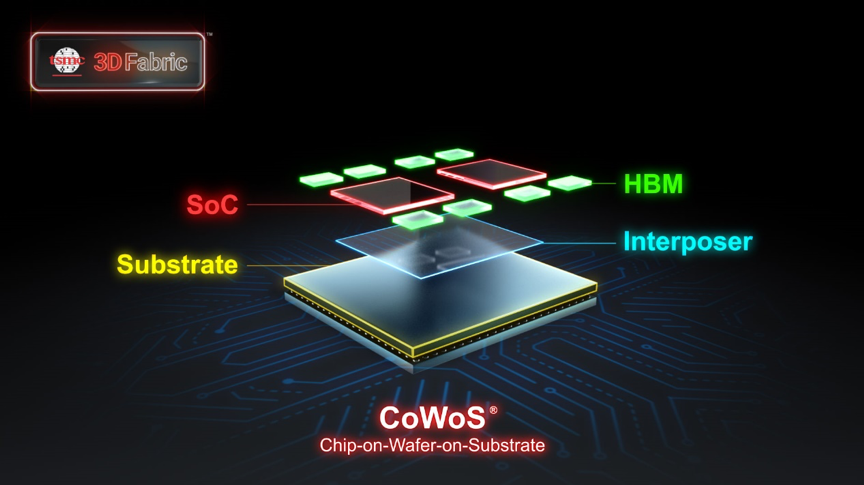
CoWoS starts with individually validated, high-yield dies, then integrates them onto a common silicon interposer, achieving chiplet-scale density without the manufacturing risk of a monolithic wafer. It is a disciplined, building-block approach, and it works. Nvidia’s Blackwell architecture is its most visible proof point, stacking compute and HBM in a tightly coupled package that delivers substantial bandwidth gains over discrete multi-chip configurations.
By using known-good-die stacking, an architect doesn’t have to commit to a full package unless and until they’re confident in each component. The end result? Heterogeneous integration that is both manufacturable and scalable.
But CoWoS doesn’t eliminate the memory wall. It just relocates it. As bandwidth between compute and memory increases, so does the appetite for data. At petabyte-scale AI workloads, the gap between how fast compute can process data and how fast memory can supply data remains the defining system constraint. And this scale means that bandwidth alone isn’t the only concern: the energy cost of moving data in picojoules-per-bit must be a first-order design consideration.
This is where the architectural choices that seem abstract become expensive. Interconnect topology, latency budgets, and bandwidth allocation can’t be revisited, let alone addressed for the first time, at physical integration. When systems span dozens of chiplets, multiple memory tiers, and complex die-to-die interconnects, a bottleneck discovered late is a bottleneck you have to live with.
The industry has adjusted to the reality of data movement as the key constraint. The real question is how to simultaneously solve it at every level of the stack. A hundred different innovations—wafer-scale fabrics, chiplet interconnects, HBM stacking, die-to-die signaling, and more—are converging on the same problem from a hundred different angles. Clearly, the next generation of systems can’t treat these as separate concerns.
Instead, architects have to comprehend interconnect topology, memory hierarchy, bandwidth allocation, and energy efficiency as parts of a united system from the earliest phases of design, not just when they become bottlenecks during physical integration.
That system-level view is precisely where Baya is focused. As the industry accelerates across both paths, we’re positioned to turbocharge that innovation by giving architects the insight to design the right data movement pathways before silicon is committed and the confidence to get complex heterogeneous systems right the first time.
Related Chiplet
- Optical Chiplet
- Reverse Gearbox Chiplet
- FlexGen Multi-Die Smart Network-on-Chip (NoC) IP
- Ncore Multi-Die Interconnect IP
- Integrated voltage regulator (IVR) chiplet
Related Blogs
- Wafer-Scale vs. Chiplets: The new war?
- 2026 Chiplet Summit: Interconnect is the New Frontier of System Performance
- Foundry 2.0 – the New Path Forward for Moore’s Law
- From Monolithic SoCs to Chiplets: A New Hardware Security Paradigm