Ultra-high repeatability and ultra-low insertion loss wafer and die-level visible-range E-PIC device characterization using an MPI Corp. probe system, enabled by process optimization from Quantum Transistors

Quantum Transistors Inc. (“QT”) pioneered an electro-optic test solution for the wafer- and die-level characterization of atom- and photon-based integrated quantum photonic circuits in the visible spectrum.
By Lawrence van der Vegt – Head of Photonics at MPI Corporation, and Thomas Ferreira de Lima – Principal Photonic Engineer, Benjamin Strekha - Photonic Designer and Igal Bayn – VP Photonics at Quantum Transistors Inc.

Quantum Transistors is a quantum computing startup developing a scalable quantum processor architecture based on solid-state spin qubits in engineered diamond structures integrated with photonic interconnects. Their approach relies on creating and controlling color centers in synthetic diamond, which act as stable quantum bits whose electron spin states can be initialized, manipulated, and read out using optical and microwave techniques. These spin qubits exhibit long coherence times and can operate at relatively higher temperatures compared to superconducting qubits. The architecture integrates these diamond qubits with on-chip integrated photonic circuits, enabling photons to mediate entanglement between spatially separated qubits. This photonic coupling allows the system to scale beyond nearest-neighbor interactions and supports modular quantum processor designs.
Unlike many other quantum architectures that face challenges in scaling, their technology offers the potential for large-scale, fault-tolerant quantum computing systems deployable in standard data-center environments, bridging the gap between laboratory prototypes and commercially viable quantum processors.
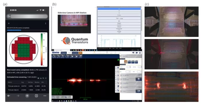
Grating, Trench and Edge coupling onto electro-optic integrated circuits in the visible spectrum. (a) Wafer level dashboard monitoring measurement progress, (b) Real-time power monitoring with SENTIO and External Power Meter. (c) Top and Side view of live edge coupler measurement.
The primary challenges associated with testing these devices stem from the need to support large-scale validation across the entire ecosystem, from development and characterization to validation, optimization, known good die identification (KGD), high-volume testing, and packaging while maintaining high throughput, precision, and repeatability in the visible wavelength range. Device and system sensitivity, along with environmental conditions, directly influence the accuracy and repeatability of measurements, which are essential for reliably determining the performance and quality of the device under test. By maintaining tight control over these factors, the testing process produces consistent, high-quality data that accurately reflects the true performance of the device.
High accuracy, repeatability, and compliance with eye-safety requirements together with the best-in-class technical support were key criteria in selecting MPI Corporation, driven by the scalable architecture of its probe and test solutions. The resulting measurement data was subsequently leveraged to refine and optimize Quantum Transistors’ Process Design Kit (PDK) and identify good dies.
A critical requirement was the system’s capability to automatically compensate for temperature variations within a ±2 °C window, while supporting continuous operation over multiple days. Equally important was the ability to pause and resume measurement sequences without impacting data integrity or system repeatability. While these requirements are generally manageable under standard conditions, the specific measurement environment introduced additional complexity. This included maintaining tight control over Polarization Extinction Ratio (PER) and Polarization Control (POL) within a single-mode fiber terminated by a lensed tip with a mode field diameter (MFD) of 1.66 µm, while achieving a mean insertion loss (IL) of 0.015 dB (σ = 0.003 dB). All these parameters were maintained with minimal alignment overhead and over several days per wafer while situated in a Midtown Manhattan office tower near a busy subway station.
To meet these stringent requirements, QT developed a dedicated test environment based on MPI’s TS3500, configured for visible wavelength operation and integrated with SENTIO®. This setup incorporated optimized optical fiber probes designed for trench, edge and grating coupling in the visible spectrum, best-in-class test instrumentation, and a highly optimized, automated software workflow that result in measurement throughput of 1min per full wavelength scan.
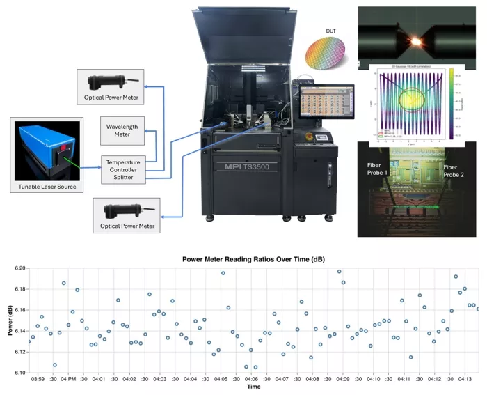
QT’s test setup and process confirmed the alignment stability of the probe system to be on par with the performance of the tunable laser.
The configuration shown above defines the measurement platform used to characterize the optical performance of QT’s grating- and edge-coupler-based E-PICs. A tunable laser provides a wavelength-dependent optical source, with the signal split into two parallel paths: one for continuous optical power and wavelength monitoring and the other for device-under-test (DUT) characterization.
The alignment subsystem supports logic-driven, fully automated optical probe positioning and DUT alignment. This is achieved by a stationary, power-stabilized, and polarization-optimized laser source in combination with a single-channel optical power meter. The analog output of the power meter is directly interfaced with the SENTIO® environment of the MPI TS3500, enabling closed-loop feedback for high-precision, automated alignment.
The dark box option provides an integrated light-isolation enclosure specifically designed for high-sensitivity electro-optical measurements. It establishes a controlled, low-stray-light environment that avoids ambient light interference and disruptive airflow, enabling accurate characterization of photonic devices. This is particularly important for measurements in the visible and near-infrared wavelength ranges, as well as for high optical power testing, while ensuring compliance with laboratory and manufacturing safety standards.
A key measurement enabled by this setup is the evaluation of optical insertion loss (IL) as a function of wavelength across the visible spectrum. This spectrally resolved analysis is critical for verifying device performance against design specifications, identifying fabrication-induced variations, and ensuring compliance with the stringent requirements of scalable, quantum-based optical and atomic systems.
Related Chiplet
- eFPGA Chiplet
- DPIQ Tx PICs
- IMDD Tx PICs
- Near-Packaged Optics (NPO) Chiplet Solution
- High Performance Droplet
Latest Blogs
- How Intel Foundry Packaging Technologies Redefine AI and HPC Scalability Limits at ECTC 2026
- From complexity to simplicity: Scaling and future-proofing chiplets with AMBA®︎ CHI C2C property negotiation
- High-Speed Heterogeneous Integration with Multiphysics Analysis for TSMC SoW-X
- Chiplet Realization Beyond the Package: Why the Next AI Bottleneck Moves to the Interposer-to-PCB Boundary
- Advancing UCIe Performance: Enabling 40G for Next-Generation Multi-Die Designs