Wooptix Targets AI Packaging Bottleneck with Astronomy Tech
A Canary Islands startup brings wavefront imaging to semiconductor metrology, aiming to tackle wafer shape challenges in 3D integration.
By Pat Brans, EETimes | May 11, 2026
As chipmakers race to build faster AI processors, attention has shifted beyond transistor scaling and toward advanced packaging, hybrid bonding, and 3D integration. That shift is creating new manufacturing bottlenecks—among them, how to precisely measure wafer shape, topography, and warpage as devices become thinner, denser, and increasingly stacked.
One company hoping to capitalize on that transition is Wooptix, a Spain-based startup whose core technology originated not in semiconductor fabs, but in astronomy labs in the Canary Islands.
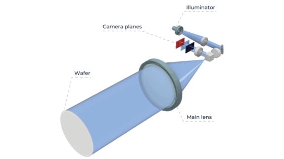
The company says wavefront-sensing techniques originally developed to correct atmospheric distortion in telescopes can now help semiconductor manufacturers inspect wafers faster and with greater detail than some conventional approaches.
To read the full article, click here
Related Chiplet
- DPIQ Tx PICs
- IMDD Tx PICs
- Near-Packaged Optics (NPO) Chiplet Solution
- High Performance Droplet
- Interconnect Chiplet
Related News
- CEA Combines 3D Integration Technologies & Many-Core Architectures to Enable High-Performance Processors That Will Power Exascale Computing
- EV Group Highlights 3D Integration Process Solutions at SEMICON Taiwan 2024
- The Basics of Chiplet Integration and Importance of Adhesive Solutions
- imec: New Methods for 2.5D and 3D Integration
Latest News
- Quantum Computing Inc. Completes Acquisition of NHanced Semiconductors, Inc.
- GlobalFoundries qualifies SLATE™ advanced packaging technology on 9SW platform for next-generation radio frequency applications
- Qnity Powers the Transition from Shrink to Stack with Advanced Packaging Solutions
- NHanced Semiconductors President Robert Patti to Deliver Plenary Presentation on the Critical Role of Advanced Packaging at the 2026 Lithography Workshop
- Intel Announces Leadership Appointment at Intel Foundry to Accelerate Development and Manufacturing