Wave Photonics Brings CSA Catapult’s Wafer-Scale PIC Testing to Its PDK Management Platform
January 21, 2026 -- Wave Photonics has made wafer-scale photonic integrated circuit (PIC) testing services from the Compound Semiconductor Applications (CSA) Catapult available through its PDK Management Platform. This gives designers working on visible to infrared wavelengths access to the design rules and test requirements required for wafer-scale PIC testing.
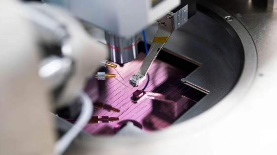 CSA Catapult has developed visible-wavelength PIC testing capabilities during the SiNQ project, an Innovate UK–supported project focused on developing integrated photonic components for quantum systems and strengthening the UK integrated photonics supply chain. While wafer-scale testing at telecom bands is widely available, this capability addresses the growing demand for PIC characterisation beyond traditional telecom wavelengths and supports emerging applications in quantum and sensing technologies.
This collaboration brings together Wave Photonics’ proprietary automated design technology, which enables rapid, fabrication-tolerant PIC development across abroad range of wavelengths from visible to infrared and material platforms, with accessible wafer-scale testing services. Making CSA Catapult’s testing services available through the platform complements this design capability by helping ensure PIC designs for visible wavelengths are developed with downstream testing requirements in mind and validated after fabrication.
Through the Wave Photonics PDK Management Platform, designers can discover CSA Catapult’s testing services, understand supported wavelength ranges, and access the relevant design rules and test requirement documentation required for wafer-prober testing. This provides a clearer and more consistent path from PIC design through to measurement and validation.
Explore the testing services: here
Caroline O’Brien, CEO of CSA Catapult, said, “We’re delighted to be working with Wave Photonics on visible and short-wavelength PIC testing, helping to support the photonics ecosystem. By developing this test service for short wavelength capability, it will meet the growing demand for advanced PIC technologies. We look forward to continuing our work with Wave Photonics on these test services and enhancing the technology further.”
James Lee, Wave Photonics CEO, said, “There is a growing need for visible-wavelength PIC testing as PIC design expands beyond telecom wavelengths. It was great to work with CSA Catapult on the SiNQ project to develop this first-of-its-kind testing capability. Combined with the SiNQ PDK on our platform, this provides designers with a more streamlined route from PIC design through to measurement and validation.”
About CSA Catapult:
The Compound Semiconductor Applications (CSA) Catapult is the UK’s authority on compound semiconductor applications and commercialisation. CSA Catapult provides access to state-of-the-art facilities and expertise for the measurement, characterisation, and validation of compound semiconductor technologies, supporting the growth of advanced photonics, electronics, and emerging semiconductor applications.
About Wave Photonics:
Wave Photonics, based in Cambridge, UK, develops cutting-edge design technology to drive the advancement and mass adoption of integrated photonics. The company uses a fabrication-aware computational model to facilitate the rapid development of PIC designs. The company empowers engineers to design their chips for a wide range of wavelengths and many challenging applications, including telecom/datacom, space-comm, sensing, quantum, optical computing, and diagnostic and healthcare sensing.
Related Chiplet
- Integrated voltage regulator (IVR) chiplet
- High-performance connectivity chiplets
- eFPGA Chiplet
- DPIQ Tx PICs
- IMDD Tx PICs
Related News
- Wave Photonics launches its PDK Management Platform with CORNERSTONE as the first user
- Wave Photonics PDKs Now Support Photonic Circuit Simulation in Cadence Spectre
- Wave Photonics Acquires Phoelex Chiplet IP to Power Datacoms & AI Growth
- Lightium, MPI Corporation, and Axiomatic_AI Announce Strategic Partnership to Revolutionize Photonic Integrated Circuit (PIC) Device Testing with AI-Driven Solutions
Latest News
- Intel and Lens Technology Collaborate to Enable Advanced Semiconductor Packaging for the AI Era
- Amkor Technology Announces Strategic Partnership with NVIDIA to Expand Advanced Packaging and Test for Next-Generation AI Infrastructure
- Synopsys Enables AMD Instinct™ MI455X GPU Design with Comprehensive Multi-Die Solution
- AI Data Centers Push Silicon Photonics Toward 300-mm Scale
- TYLsemi De-Risks Chiplets With New Business Model