As Chips Go Vertical, Metrology Struggles to Keep Up
Advanced-node manufacturing is pushing semiconductor inspection beyond traditional top-down measurement and toward reconstructing buried 3D structures that conventional tools can no longer easily see.
By Pat Brans, EE Times | June 9, 2026
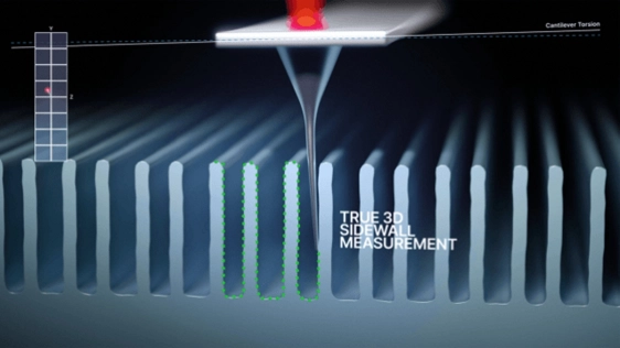
Semiconductor inspection has traditionally meant looking down. Optical metrology and critical dimension scanning electron microscopy (CD-SEM) systems were optimized for lateral scaling, where the central challenge was shrinking dimensions across the surface of silicon. That approach worked when transistor architectures remained relatively planar and accessible.
Today, however, advanced-node manufacturing is moving increasingly into the Z-axis. Gate-all-around transistors, recessed nanosheets, HBM memory, vertically stacked NAND, hybrid bonding, and future CFET architectures are creating structures that are narrower, deeper, and more difficult to inspect. Critical variability increasingly exists along buried sidewalls and recessed regions rather than only on the top surface of the device.
“Scaling is no longer happening only in the X-Y plane, but increasingly in the Z direction,” Philippe Leray, VP of advanced patterning at imec, told EE Times. “More and more, we need to look deep inside these structures to characterize defects, composition, roughness, and dimensional variation.”
To read the full article, click here
Related Chiplet
- Integrated voltage regulator (IVR) chiplet
- High-performance connectivity chiplets
- eFPGA Chiplet
- DPIQ Tx PICs
- IMDD Tx PICs
Related News
- CHIPS for America Announces up to $300 million in Funding to Boost U.S. Semiconductor Packaging
- Biden-Harris Administration Announces Arizona State University Research Park as Planned Site for Third CHIPS for America R&D Flagship Facility
- AI Boom Drives Demand for Ultra-Large Packaging as ASICs Expected to Shift from CoWoS to EMIB, Says TrendForce
- Vertical Compute raises €57M to solve the AI memory bottleneck with new high density memory
Latest News
- Amkor Technology Announces Strategic Partnership with NVIDIA to Expand Advanced Packaging and Test for Next-Generation AI Infrastructure
- Synopsys Enables AMD Instinct™ MI455X GPU Design with Comprehensive Multi-Die Solution
- AI Data Centers Push Silicon Photonics Toward 300-mm Scale
- TYLsemi De-Risks Chiplets With New Business Model
- Cadence Introduces AuraStack AI Super Agent, the World’s First Agentic AI Platform for PCB and Advanced Packaging