CoAsia SEMI Unveils Advanced Strategy for Next-Generation Chiplet Platform 'CoCs™' at Samsung SAFE Forum
June 10, 2026 -- CoAsia SEMI (CEO Shin DS) unveiled its advanced packaging strategy and future roadmap for its next-generation chiplet packaging platform, 'CoCs™ (CoAsia Chiplet Solution),' at Samsung Foundry's 'SAFE™ Forum 2026' held in Silicon Valley, USA.
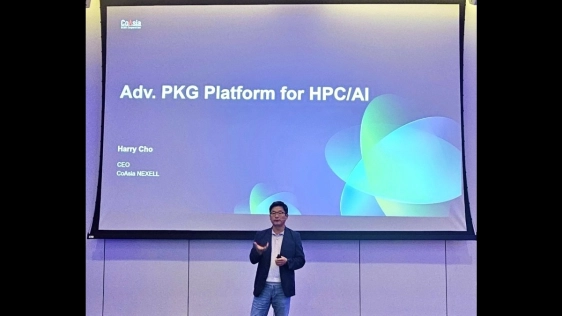 With the recent expansion of the AI and HPC markets, the limitations of large-scale chip (Big Die) design have emerged as a core industry challenge. Amidst this, CoAsia SEMI presented a solution at the forum that streamlines the development of next-generation chiplets capable of simultaneously securing performance, yield, and power efficiency.
CoAsia SEMI's CoCs™ is a platform that divides a single chip into functional dies and applies the optimal process and packaging structure to each die. By standardizing and modularizing the chiplet structure design and advanced packaging implementation processes, it enables faster and more stable development of AI and HPC semiconductors tailored to customer requirements. It supports high-bandwidth memory including HBM3E and the latest high-speed interfaces such as UCIe, PCIe, and SerDes, optimizing the ultra-high-speed data processing and integration required for high-performance AI and HPC semiconductors.
CoAsia SEMI announced that it has made it possible to shorten development timelines and reduce manufacturing costs by verifying over 200 items in the pre-simulation stage during the SI/PI (Signal and Power Integrity) verification process—which is considered a core challenge in chiplet design—and by applying standardized methodologies for each project.
In this presentation, CoAsia SEMI also revealed its roadmap for 3D package solutions based on SoC and memory die stacking, going beyond RDL and interposer-based 2.3D/2.5D structures. The strategy is to gradually expand high-speed interface IPs such as LPDDR, MIPI, PCIe, and UCIe, along with HBM platforms, in line with Samsung Foundry's advanced processes. The company plans to continuously upgrade its next-generation package structures to respond effectively to the demands of the AI and HPC markets.
In this regard, the 3D package solution is scheduled to undergo sample verification in the second quarter and enter mass production in the third quarter, while the sample out of the 2.5D chiplet platform is also being pushed for within this year.
On the business side, CoAsia SEMI is establishing a cooperative system with top-tier global OSAT companies such as Amkor and ASE, centered around Samsung Foundry. Based on an integrated supply chain management system that encompasses interposer and substrate design, connection with packaging and material companies, and mass production, the company has also equipped itself with full end-to-end execution capabilities.
Shin Dong-soo, CEO of CoAsia SEMI, stated, "In the AI and HPC era, integrated solution capabilities—which include advanced packaging and supply chain response capabilities beyond simple design capabilities—are becoming increasingly crucial." He added, "Based on CoCs™, we will continue to strengthen our competitiveness in the next-generation chiplet sector within the Samsung SAFE™ ecosystem."
Related Chiplet
- Optical Chiplet
- Reverse Gearbox Chiplet
- FlexGen Multi-Die Smart Network-on-Chip (NoC) IP
- Ncore Multi-Die Interconnect IP
- Integrated voltage regulator (IVR) chiplet
Related News
- CoAsia SEMI and Rebellions Join Forces to Jointly Develop Next-Generation AI Chiplet Based on REBEL
- Alphawave Semi Delivers Cutting-Edge UCIe™ Chiplet IP on TSMC 3DFabric® Platform
- CoAsia SEMI Announces AI Chiplet Production Collaboration With Tenstorrent
- Synopsys Advances Power and Performance for AI and Multi-Die Designs on Latest Samsung Foundry Processes at SAFE Forum 2026
Latest News
- Amkor Technology and NVIDIA Advance Strategic Partnership for AI Infrastructure
- Siemens expands agentic AI collaboration to tackle 3D IC power and thermal challenges with NVIDIA
- Photon Bridge Raises €10M to Tackle AI’s Emerging Laser Bottleneck
- Abacus Semiconductor and Aalto University Announce Research Cooperation on High-Speed Chiplet Interconnects
- UK Launches Semiconductor Catapult to Strengthen Sovereign Capabilities in AI Hardware and Defence