Who Owns the Interface When Chiplets Come from Different Suppliers?

Why interoperability must extend from electrical standards to physical manufacturing evidence
The promise of a multi-vendor chiplet ecosystem
The chiplet industry is moving toward a future in which semiconductor companies can assemble complex systems from independently developed components.
A compute chiplet from one supplier, an I/O chiplet from another, and a specialized accelerator from a third could potentially be integrated into a common advanced package.
The advantages are clear: greater architectural flexibility, technology-node optimization, design reuse, and reduced dependence on a single supplier.
Industry standards such as Universal Chiplet Interconnect Express (UCIe) are helping make this vision possible by establishing common electrical and protocol interfaces.
But there is a manufacturing question that interoperability alone cannot answer.
What happens when two compliant chiplets are integrated into a package and the assembled interface fails?
Both suppliers may have delivered components that meet their individual acceptance criteria.
The package assembler may have followed its qualified process.
Yet the completed product may still exhibit insufficient signal margin, excessive thermal sensitivity, or intermittent interconnect failures.
The problem is not necessarily that any individual component was manufactured incorrectly.
It may be that the physical boundary between components was never qualified adequately as a complete system.
1. Electrical compatibility is not the same as physical integration
Consider two chiplets designed to communicate over a standardized die-to-die interface.
Each passes its individual electrical tests. Their protocols are compatible, and both satisfy the applicable interface specifications.
During packaging, however, the final connection depends on additional physical conditions.
Die placement, bump geometry, interconnect height, substrate warpage, bonding quality, and temperature all influence the realized interface.
These factors can interact.
A small placement deviation may be acceptable on its own. Substrate warpage may also remain within its specified limit. But their combined effect, together with thermal expansion and interconnect variation, may consume enough margin to affect the assembled interface.
The result can be a product that passes individual component tests but fails system-level verification.
This distinction is especially important in advanced 2.5D and 3D integration, where high-density interconnects introduce tighter physical constraints and may become inaccessible after assembly.
An interface is not simply a connection between two compliant designs. It is a physical structure created by a manufacturing process.
That physical structure must be characterized, controlled, and verified.
2. Three approaches to managing the interface
There are three practical approaches, each with different benefits and limitations.
Approach A: Control the complete integration stack
One organization defines the chiplets, package architecture, manufacturing processes, and system-level acceptance criteria.
This gives the integrator direct control over interface specifications, process margins, and failure analysis.
The benefit is clear ownership and the ability to optimize the complete design and manufacturing flow.
The limitation is reduced supplier flexibility and potentially greater development cost.
This approach works particularly well when performance requirements justify tightly coordinated design and manufacturing.
Approach B: Standardize chiplet interfaces
Industry standards create common electrical and protocol requirements that allow independently developed chiplets to communicate.
UCIe is an important example. Its evolution has expanded beyond basic data communication to include capabilities for test, debug, manageability, and lifecycle support.
Standardization can reduce integration barriers and improve ecosystem flexibility.
But compliance does not automatically guarantee acceptable behavior under every package geometry, manufacturing process, thermal environment, or system configuration.
The standard establishes important interoperability requirements. The selected implementation still needs to be qualified in its intended physical environment.
Approach C: Establish a shared physical acceptance envelope
A third approach combines standardized interfaces with explicit agreement on the physical conditions and evidence required for successful integration.
Rather than relying only on individual component acceptance, the participating suppliers and system integrator define an interface qualification envelope.
This may include placement accuracy, interconnect geometry, channel characteristics, thermal conditions, mechanical deformation, and corresponding electrical performance margins.
The envelope should also establish which measurements are required, when they are taken, and how deviations are evaluated.
Its advantage is that the integration problem becomes measurable before a failure occurs.
Its limitation is the need for additional coordination, shared data, test development, and potentially tighter supplier qualification.
These three approaches are not mutually exclusive. A vertically integrated manufacturer may still use industry standards, while a multi-vendor ecosystem may require different qualification envelopes for different packaging technologies.
3. From supplier compliance to manufacturing evidence
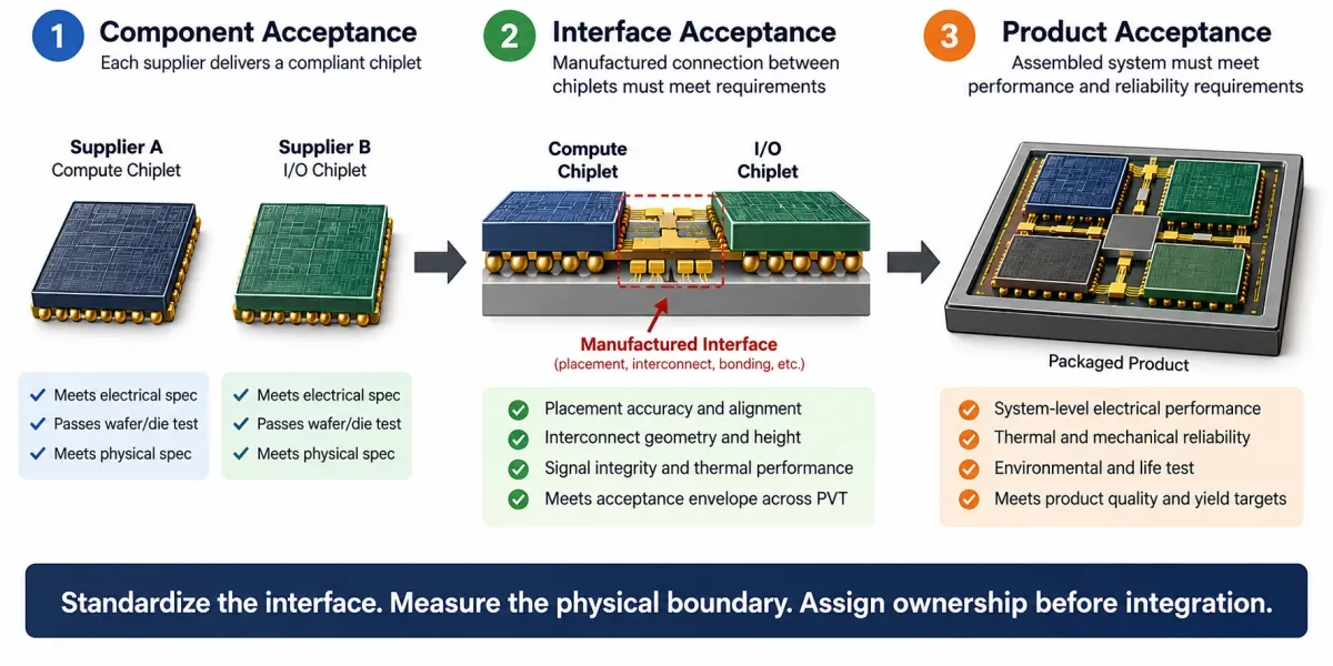
The key is to distinguish three types of acceptance.
Component acceptance: Does each chiplet meet its defined requirements before integration?
Interface acceptance: Does the manufactured physical connection retain sufficient margin under specified operating and environmental conditions?
Product acceptance: Does the completed system meet its performance, reliability, and quality requirements?
Each answers a different engineering question.
Known-good-die screening addresses the first. Package metrology, interconnect characterization, and post-assembly testing contribute to the second. System validation and reliability qualification establish the third.
The challenge is connecting the evidence.
For example, an assembled product may show an increase in link errors at elevated temperature.
Electrical testing identifies the symptom. Physical inspection may reveal interconnect geometry variation. Process history may indicate a particular bonding or assembly condition.
Connecting those observations allows engineers to determine whether the problem originated in the die, package, process, or interaction among them.
Without this connection, suppliers may have individually acceptable data but insufficient evidence to determine the actual failure mechanism.
This is where multi-vendor manufacturing requires more than interface specifications.
It requires traceable evidence of what was built and how the resulting interface performs.
4. Assigning ownership before integration
Supplier quality agreements and manufacturing responsibility matrices are well-established industrial practices.
The opportunity is to apply that discipline directly to the physical boundaries of heterogeneous chiplet systems.
Before integration, the participants should establish:
- Who defines and approves the interface acceptance envelope?
- Who supplies and validates the necessary physical and electrical measurements?
- Who owns diagnosis when individual components pass but the assembled interface fails?
- Who has authority to change interface specifications, assembly processes, or acceptance limits?
- Who establishes final product qualification and release criteria?
These are not merely contractual questions.
They determine what data must be collected, what tests must be designed, and how rapidly a manufacturing problem can be isolated and corrected.
A technically compliant chiplet is not necessarily interchangeable across every manufacturing environment.
True interchangeability requires compatibility at the electrical, physical, manufacturing, and product levels.
The manufacturing decision
The objective should not be to eliminate supplier boundaries or force every company into one integration model.
Multi-vendor chiplets offer meaningful advantages in innovation, scalability, and supply-chain flexibility.
The objective is to ensure that the physical interfaces created by that flexibility remain measurable, repeatable, and accountable.
Standardized communication interfaces are an essential foundation.
But the long-term success of an open chiplet ecosystem will also depend on whether suppliers and integrators can establish shared physical acceptance criteria, preserve manufacturing traceability, and resolve integration failures using engineering evidence.
The industry does not simply need chiplets that can communicate. It needs chiplets that can be integrated into reliable products repeatedly, across suppliers and manufacturing environments.
Moh's Golden Rule:
Standardize the interface. Measure the physical boundary. Assign ownership before integration.
© 2026 Dr. Moh Kolbehdari. All rights reserved.
Related Chiplet
- Optical Chiplet
- Reverse Gearbox Chiplet
- FlexGen Multi-Die Smart Network-on-Chip (NoC) IP
- Ncore Multi-Die Interconnect IP
- Integrated voltage regulator (IVR) chiplet
Related Blogs
- From horsepower to high-performance compute: automotive chiplets take the leap towards autonomous edge computing
- Prototyping Chiplets from the Desktop!
- Four Reasons Chiplets Will Take Over the World (and why it hasn’t happened yet)
- Synopsys-Ansys 2.5D/3D Multi-Die Design Update: Learning from the Early Adopters
Latest Blogs
- Who Owns the Interface When Chiplets Come from Different Suppliers?
- Q&A: Bringing Co-Packaged Optics to AI Infrastructure
- Notes From OCP: Agnostic on the Package, Practical About the Laser
- Lam and imec Expand Collaboration to Advance Manufacturability of Next-Gen 3D Integration Technologies, Explore Aether Dry Resist Use Cases
- AI Memory Is More Than HBM: The Chiplet Era Is Forcing the Entire Memory Hierarchy to Scale