Silicon Motherboard Enables Double-Sided Integration of ICs and Passive Components

Nisshinbo Micro Devices developed Silicon Motherboard (Si-MB), a novel 3D packaging technology. By mounting ICs and external components on both sides of a small silicon substrate and enclosing them in a single package, this technology significantly reduces the mounting area. This kind of innovative advancement is poised to significantly contribute to downsizing devices and systems.
Increasing demand for smaller, higher density designs
 The number of semiconductors deployed across a wide range of devices and systems, including automobiles, industrial equipment, and consumer electronics, continues to rise steadily. Concurrently, the overarching push to shrink overall device sizes has created increasingly stringent constraints on the available mounting area. As a result, manufacturers are now under immense pressure to achieve further miniaturization and higher integration of components, all while maintaining absolute reliability under harsh operating conditions. As the number of components increases, the supply chain becomes more complex, and procurement risks increase, making the reduction of the bill of materials (BOM) another critical objective.
To meet these demands, Nisshinbo Micro Devices developed Silicon Motherboard (Si-MB)*.
*“Si-MB” is a registered trademark of Nisshinbo Micro Devices.
Mounting ICs and passive components on both sides of the substrate
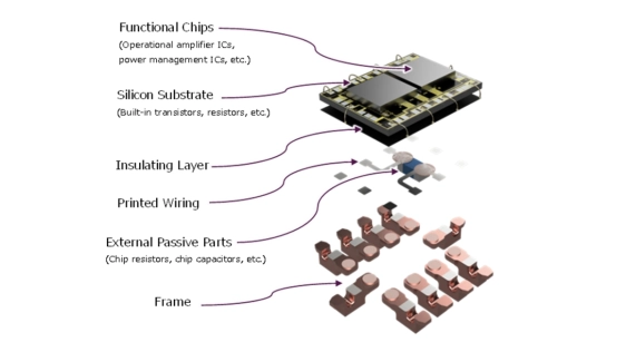
Silicon Motherboard is a 3D packaging technology that integrates ICs and electronic components in which circuits are formed on both sides of a silicon substrate, and the entire assembly is enclosed within a single package.
Transistors, resistors, and capacitors are first formed inside the silicon substrate using a wafer fabrication process. Functional chips, such as operational amplifier ICs and power management ICs, are then mounted on the top surface of the substrate. External passive components that are difficult to integrate into an IC, such as chip resistors and chip capacitors, are then mounted on the printed wiring on the bottom (back) surface of the substrate. Finally, this silicon substrate is housed in commonly used packages of SOP, QFN, and SON. This approach allows for higher component density by consolidating components while using existing packages.
To read the full article, click here
Related Chiplet
- Optical Chiplet
- Reverse Gearbox Chiplet
- FlexGen Multi-Die Smart Network-on-Chip (NoC) IP
- Ncore Multi-Die Interconnect IP
- Integrated voltage regulator (IVR) chiplet
Related Blogs
- Testing At The Speed Of Light: Enabling Scalable Optical Testing For Silicon Photonics And CPO
- Advancing High‑Performance Silicon Photonics and Silicon Germanium (SiGe) for the Next Era of Optical Connectivity
- Lam and imec Expand Collaboration to Advance Manufacturability of Next-Gen 3D Integration Technologies, Explore Aether Dry Resist Use Cases
- Driving the Development and Deployment of Chiplets in the Automotive Industry