The Economics of a Failed Chiplet Package

Why chiplet modularity depends on assembly sequence, defect detection, and the cost of delivering a good package
Chiplets are changing how advanced semiconductor systems are designed. Instead of integrating every function into one large die, designers can partition compute, memory, I/O, and specialized accelerators into smaller components, potentially manufactured using different technologies and integrated within a common package.
The architectural advantages are compelling. Smaller dies may improve wafer utilization, support technology-node specialization, enable design reuse, and allow different functions to evolve independently.
But the benefits of modular design introduce a manufacturing question that deserves equal attention:
What happens to the economics of a chiplet-based system when one component fails after the rest of the package has already been assembled?
A defective chiplet identified during wafer testing may result in the loss of one component. The same defect discovered after expensive compute dies, high-bandwidth memory, an interposer, and multiple assembly operations have been combined may put the entire package at risk.
The cost of a defect therefore depends not only on its occurrence, but on when it is detected, how much manufacturing value has already been added, and whether the affected assembly can be recovered.
This makes defect detection and assembly sequencing architectural decisions, not merely manufacturing details.
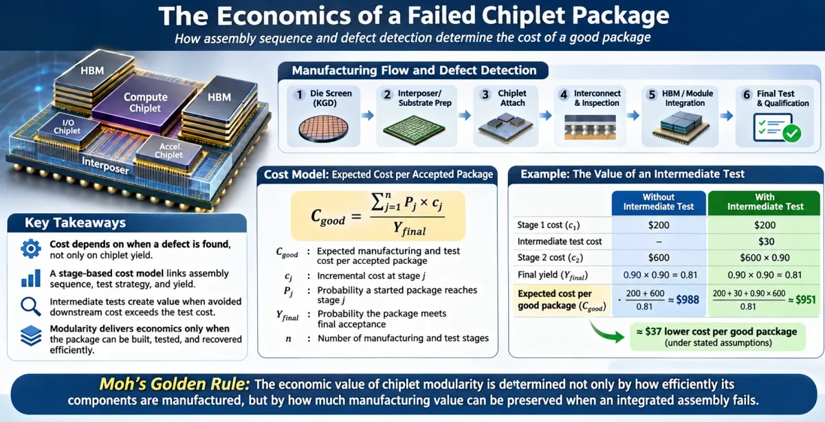
1. The Difference Between Chiplet Yield and Package Economics
Chiplet-based systems are often evaluated through the manufacturing benefits of dividing a large monolithic die into smaller components.
A smaller die may have a higher wafer fabrication yield, depending on defect density, die area, process characteristics, and the relevant failure mechanisms.
However, semiconductor manufacturing does not end when the individual chiplets pass wafer-level testing.
The components must be attached, interconnected, encapsulated or otherwise protected, thermally integrated, and tested as a functioning system.
Each operation introduces additional manufacturing conditions and possible failure mechanisms.
A package containing individually tested chiplets can still fail because of bonding defects, interconnect opens or shorts, die displacement, substrate defects, warpage, thermal-interface problems, or electrical interactions that cannot be fully evaluated before integration.
The important distinction is that the yield of individual components and the cost of producing an accepted integrated package are different engineering quantities.
A package may use chiplets with excellent preassembly test results while still experiencing expensive losses during later manufacturing operations.
The economic challenge is to account for both the probability of failure and the manufacturing value exposed when that failure becomes detectable.
2. Why the Timing of Defect Detection Matters
Consider a hypothetical AI package incorporating compute chiplets, HBM stacks, an advanced interposer, and a thermal-management assembly.
The manufacturing process may involve multiple stages:
- Screening individual dies and memory components.
- Preparing the substrate or interposer.
- Attaching selected chiplets.
- Forming and inspecting interconnects.
- Integrating additional memory and package components.
- Completing thermal and mechanical assembly.
- Performing final electrical and system-level testing.
These stages do not necessarily occur in the same order for every packaging technology.
Some processes provide opportunities to inspect or electrically test a partially assembled structure. Other processes leave important interfaces inaccessible until final integration.
This creates three possible detection outcomes.
Early detection: A defect is identified before substantial additional manufacturing value is committed.
Intermediate detection: A defect is identified after some assembly operations but before more expensive components or processes are introduced.
Late detection: A defect is found only after most or all of the package has been assembled.
The same defect can have very different economic consequences across these outcomes.
For example, an interconnect defect detected before HBM attachment may allow a defective subassembly to be rejected without consuming additional memory components. If the same defect is discovered only during final system testing, those components may already be part of an unrecoverable assembly.
Early detection is not automatically better in every case, however. Additional inspection and testing have costs, and not every defect can be observed at an intermediate stage.
The relevant engineering question is whether the value of avoiding downstream losses exceeds the cost and limitations of the additional test.
3. A More Useful Cost Model
Rather than assuming that total package yield is simply the product of identical individual-chiplet yields, manufacturing economics can be evaluated through the sequence of operations required to produce an accepted package.
For a simplified assembly process with no rework, define:
Equation (1) — Expected Cost per Accepted Package
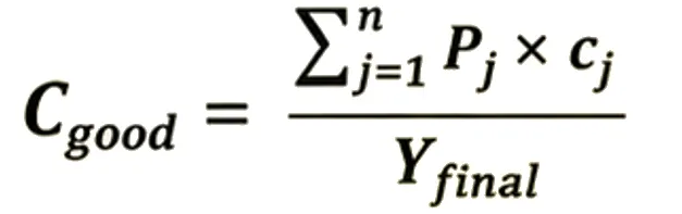
where:
- Cgood is the expected manufacturing and test cost per accepted package.
- cj is the incremental cost incurred when a package enters manufacturing stage j.
- Pj is the probability that an initially started package reaches stage j.
- Yfinal is the probability that an initially started package ultimately satisfies final acceptance criteria.
- n is the number of defined manufacturing and testing stages.
The numerator represents the expected manufacturing expenditure per started package.
The denominator accounts for the fraction of started packages that become accepted products.
Importantly, the model does not require chiplet failures to be independent or have identical probabilities.
The stage-reaching and final-acceptance probabilities may be estimated from actual manufacturing data, including interactions among failure mechanisms, provided the process stages and populations are defined consistently.
The model does require careful cost accounting. Component costs, inspection costs, and assembly costs must be assigned to the stages where they are incurred without double counting.
It also assumes that an assembly follows a defined manufacturing sequence without rework. If repair, replacement, retesting, or alternative process routes are available, those paths must be represented explicitly.
The value of this approach is that it connects three factors often considered separately: manufacturing sequence, defect detection, and the cost of acceptable production.
4. When an Intermediate Test Pays for Itself
Consider a simplified two-stage manufacturing process.
The first stage costs $200 per started package. The second stage adds $600 in components and assembly operations.
Suppose 90% of packages satisfy the first-stage conditions, and 90% of those also satisfy the remaining conditions for final acceptance.
Assume failures are nonrecoverable and that the first-stage failure population would otherwise remain undetected until final test.
Without an intermediate screen, every started package incurs both costs.
Equation (2) — Without Intermediate Screening
C_good,no screen = ($200 + $600) / (0.90 × 0.90)
C_good,no screen = $800 / 0.81 ≈ $988
Now consider adding a hypothetical $30 intermediate test that correctly identifies all first-stage failures before the $600 downstream investment.
Only 90% of started packages proceed to the second manufacturing stage.
Equation (3) — With Intermediate Screening
C_good,with screen = [$200 + $30 + (0.90 × $600)] / (0.90 × 0.90)
C_good,with screen = $770 / 0.81 ≈ $951
The intermediate test reduces expected manufacturing cost by approximately $37 per accepted package under the stated assumptions.
This is a hypothetical illustration, not a measured industry cost or yield estimate.
The economic benefit arises because the test prevents additional expensive processing of assemblies that cannot become accepted products.
But the conclusion changes if testing is more expensive, fails to detect relevant defects, incorrectly rejects good assemblies, or introduces new handling risks.
A more realistic analysis must account for test sensitivity, false rejects, test throughput, equipment utilization, and changes to downstream acceptance probabilities.
The important result is not the numerical saving.
It is that a test creates economic value when the downstream manufacturing cost it avoids exceeds its own cost and adverse consequences.
5. Three Manufacturing Strategies
The economics of a chiplet package depend heavily on how its design supports defect detection and manufacturing decisions.
Strategy A: Maximize Known-Good-Die Screening
The first strategy is to increase defect detection before assembly.
Known-good-die screening attempts to establish that each chiplet meets its required electrical and functional characteristics before integration.
This can reduce the probability of attaching a defective component to an expensive package.
However, wafer-level test access is not equivalent to full-package operating conditions.
Some interface characteristics may require neighboring chiplets, package interconnects, realistic power delivery, or thermal conditions that are unavailable during preassembly testing.
Increasing preassembly coverage can also require additional design-for-test structures, probe resources, equipment time, and test development.
The engineering tradeoff is between greater confidence in the individual component and the cost of obtaining that confidence.
Strategy B: Add Tests at Selected Assembly Stages
The second strategy is to introduce inspection or electrical tests between major assembly operations.
This can be particularly valuable before attaching expensive components or completing operations that make earlier structures inaccessible.
For example, a partially assembled package may be inspected for die position, interconnect quality, or structural defects before subsequent integration.
Where electrical access is available, selected functional or interface tests may be possible.
The challenge is determining which defects can actually be observed at each stage.
An inspection method may detect geometric abnormalities without proving electrical functionality. A limited electrical test may detect opens and shorts while missing failures that emerge under full operating conditions.
Testing must therefore be selected according to defect mechanisms, coverage, accessibility, and economic value.
Strategy C: Design for Recovery and Repair
The third strategy is to reduce the loss associated with a detected defect.
Some architectures may support redundancy, repairable memory elements, alternate routing, or replacement of selected components.
Other advanced packaging technologies, particularly fine-pitch interconnect and direct bonding approaches, may severely restrict practical rework.
Recovery also introduces its own risks.
Removing or replacing a component can affect neighboring structures, surface integrity, thermal interfaces, and long-term reliability.
A repair operation is economically valuable only when it produces a reliably acceptable assembly at lower expected cost than rejection and replacement.
Therefore, repairability cannot be assumed solely because a system is described as modular.
Design modularity and manufacturing recoverability are not the same thing.
6. Why Assembly Sequence Becomes an Architectural Variable
The manufacturing sequence determines when materials, components, and process costs are committed.
It also determines which interfaces remain accessible for inspection, testing, or repair.
Consider two possible assembly approaches.
In the first, expensive components are attached early, followed by several interconnect and packaging operations.
In the second, selected lower-cost assembly steps and their associated inspections are completed before introducing the most expensive components.
If the earlier operations contain detectable failure mechanisms, the second sequence may reduce expected loss.
However, assembly order cannot be selected from economics alone.
Physical integration imposes constraints involving alignment accuracy, bonding temperature, material compatibility, interconnect density, thermal processing, mechanical deformation, and equipment capabilities.
An economically attractive sequence may be physically infeasible or may introduce reliability problems.
The engineering objective is therefore to identify a manufacturable assembly sequence that balances defect exposure, testing opportunities, process feasibility, and final product performance.
This is why package architecture and manufacturing strategy should be evaluated together.
7. The Multi-Vendor Challenge
Chiplet ecosystems introduce another layer of complexity because design, fabrication, testing, packaging, and product validation may involve different organizations.
A logic chiplet supplier may provide wafer-level electrical results. A memory supplier may provide tested HBM stacks. A packaging organization may control interposer fabrication, die placement, bonding, and thermal assembly.
Each organization may demonstrate compliance with its own requirements.
But the final package contains interfaces and physical interactions that may not be fully represented in any individual supplier's test environment.
For example, a chiplet may pass its electrical screening while an assembled die-to-die interface fails because of geometric misalignment, interconnect defects, or operating conditions outside the preassembly test envelope.
The economic problem becomes more difficult when the failed package contains components supplied by several organizations.
Who owns the test coverage gap? Which evidence establishes that a component was acceptable before assembly? How is an assembly-induced defect distinguished from a latent component defect?
These questions connect directly to manufacturing economics because defect attribution influences supplier quality, warranty exposure, rework decisions, and the cost of recurring failure.
The solution is not necessarily more testing by every supplier.
It is a clearer engineering definition of what each test demonstrates, which defects remain undetected, and which integration stages carry responsibility for resolving them.
8. The Manufacturing Decision Is Broader Than Yield
Yield is important, but it is not sufficient to determine whether a chiplet manufacturing approach is economically attractive.
Two processes can achieve the same final acceptance yield while incurring different costs.
One may reject defective assemblies early. The other may discover equivalent defects only after expensive components and manufacturing operations have been added.
Likewise, a process with more testing may appear more expensive per started package while producing accepted packages at lower overall cost.
The correct evaluation should consider the manufacturing cost of accepted output, the value committed at each stage, test coverage, assembly feasibility, recoverability, and the consequences of undetected defects.
As advanced AI packages integrate more chiplets, memory stacks, high-density interconnects, and specialized structures, these manufacturing decisions become increasingly consequential.
The architectural question is no longer simply whether smaller chiplets improve fabrication economics.
It is whether the complete integration strategy produces acceptable packages with a manageable combination of cost, yield, performance, and reliability.
9. From Component Modularity to Manufacturing Modularity
Chiplet technology offers a compelling path toward reusable semiconductor building blocks.
But a reusable design component does not automatically become a low-cost manufacturing building block.
For modularity to create sustained economic value, the physical architecture must also support the appropriate manufacturing sequence, test accessibility, defect detection, and qualification strategy.
A highly integrated package may deliver excellent performance while remaining expensive to produce because failures are detected too late.
A different package architecture may sacrifice some theoretical optimization while achieving more predictable assembly, better test coverage, or lower loss of valuable components.
The preferred choice depends on the actual engineering and economic constraints.
The next phase of chiplet industrialization will require closer coordination among design teams, test engineers, packaging specialists, manufacturing organizations, and product integrators.
Not simply to increase the yield of each chiplet, but to ensure that the complete package can be manufactured and accepted at a sustainable cost.
Moh's Golden Rule: The economic value of chiplet modularity is determined not only by how efficiently its components are manufactured, but by how much manufacturing value can be preserved when an integrated assembly fails.
Related Chiplet
- Optical Chiplet
- Reverse Gearbox Chiplet
- FlexGen Multi-Die Smart Network-on-Chip (NoC) IP
- Ncore Multi-Die Interconnect IP
- Integrated voltage regulator (IVR) chiplet
Related Blogs
- OCP Open Chiplet Economy is Leading the Next Wave of AI: Inference
- Chiplet Realization Beyond the Package: Why the Next AI Bottleneck Moves to the Interposer-to-PCB Boundary
- The Chiplet Is Not the System: Partitioning, Placement, and Package Geometry in Heterogeneous Integration
- Chiplet Modularity Is Becoming Part of the AI Architecture