Ceramic Substrates for Advanced Semiconductor Packaging: Benefits and Applications

As semiconductor devices become smaller, more powerful, and increasingly integrated, the substrate beneath them is taking on a more important role.
 For decades, organic laminates have been the mainstream choice for electronic packaging because they offer cost advantages, routing density, and scalability. Ceramic substrates, however, never disappeared. They remained essential in applications where thermal performance, dimensional stability, hermeticity, and long-term reliability mattered more than cost alone.
Now, heterogeneous integration is bringing many of those same requirements into newer applications.
From high-power GaN and SiC devices to MEMS, medical devices, aerospace systems, and advanced 2.5D and 3D architectures, ceramic substrates are increasingly being considered as more than a specialized packaging material. They can provide a combination of electrical, mechanical, thermal, and environmental characteristics that conventional organic substrates cannot always deliver.
Ceramic vs. Organic Substrates for Advanced Packaging
The original advantages of ceramic packaging are well established.
Ceramics can provide excellent hermeticity and long-term reliability, strong RF and microwave performance, and a coefficient of thermal expansion (CTE) that more closely matches semiconductor materials such as silicon, GaN, and GaAs. These characteristics made ceramic packaging particularly valuable in aerospace, defense, radar, RF, and other extreme-environment applications.
Organic substrates ultimately became dominant in higher-volume applications because of their lower cost and greater routing density. Ceramic remained where reliability requirements were especially demanding.
The difference today is that several new pressures are making those ceramic characteristics relevant to a much broader range of advanced electronic systems.
Key Benefits of Ceramic Substrates
CTE Matching and Reliability in Semiconductor Packaging
Thermal expansion becomes increasingly important as devices become smaller while handling greater amounts of power.
Silicon has a CTE of approximately 2.6 ppm/K, while conventional FR-4 materials are typically around 14–17 ppm/K. That difference can create mechanical stress during repeated temperature cycling.
Aluminum nitride (AlN), by comparison, has a CTE of approximately 4.6–4.8 ppm/K, making it much closer to silicon and other semiconductor materials.
That closer match can help reduce thermomechanical stress at interfaces, particularly in applications involving high-power devices and repeated thermal cycling.
The requirement is not new. What is changing is where it matters.
As heterogeneous integration puts more functionality and power into smaller packages, controlling the mechanical effects of thermal expansion becomes increasingly important.
Low Outgassing and Reliability Benefits of Ceramic Packaging
Ceramics also offer characteristics that are particularly valuable in sealed, vacuum, and high-reliability environments.
Modern applications are expanding the need for low-outgassing packaging beyond traditional aerospace and defense applications. MEMS devices, medical systems, and space payloads can all require packaging materials that maintain a controlled environment over long periods.
For example, ASTM E595 establishes limits for total mass loss and condensable volatile residue in applications where outgassing is a concern.
MEMS devices can be especially sensitive. Resonant MEMS structures may require vacuum packaging to maintain their performance, making the package itself an important part of the device architecture.
Ceramic packaging can provide a path toward hermetic, low-outgassing structures while supporting increasingly complex electrical interconnects.
Thermal Management for GaN and SiC Power Electronics
Perhaps the most significant driver is heat.
The transition toward GaN and SiC power devices, combined with increasingly dense 2.5D and 3D architectures, is concentrating more power into smaller areas.
AlN is particularly interesting because of its thermal conductivity, which can range from approximately 150–240 W/m·K. That is roughly an order of magnitude higher than alumina.
For high-power electronics, the ability to move heat away from the die is not simply a packaging consideration. It can directly influence system performance, reliability, and design flexibility.
As AI and high-performance computing systems push power density higher, thermal management becomes increasingly difficult to solve at the board level alone.
The Submount Problem
One challenge is that simply adding a ceramic submount beneath a high-power device does not necessarily capture all of the benefits of ceramic.
A typical architecture may place a GaN or SiC die on an AlN submount, which is then attached to an organic PCB. This provides a high-performance thermal path immediately beneath the device, but it also introduces another level of interconnection.
Instead of one interconnect system, the design now has multiple interfaces between the die, ceramic submount, and PCB.
Those interfaces introduce additional thermal resistance, solder joints, wire bonds, and opportunities for CTE mismatch.
For example, AlN has a CTE of approximately 4.6–4.8 ppm/K, compared with approximately 14–17 ppm/K for FR-4. During thermal cycling, the resulting difference in expansion can place additional stress on solder joints.
This creates an interesting design question: if the ceramic is already providing the thermal and mechanical advantages the device needs, why stop at the submount?
Moving Toward Ceramic-Based System Integration
One potential path is to move more of the electronic assembly onto the ceramic itself.
Instead of treating the ceramic as a small submount beneath an individual device, a ceramic substrate can become a larger part of the package architecture.
This can take several forms.
A monolithic ceramic approach can place multiple components directly on a ceramic thermal platform, allowing the ceramic to function as both an electrical substrate and heat spreader.
Another approach is a ceramic system-in-package (SiP), where power devices, drivers, passives, and other supporting circuitry are integrated into a ceramic package before being attached to the main PCB.
This architecture can retain the thermal advantages of the ceramic while freeing PCB area for other system functions. It also creates an opportunity to test a completed SiP before it is integrated into the larger system.
The concept is not entirely new. Power modules already demonstrate the value of combining switches, drivers, and other functions into factory-tested assemblies.
Ceramic Substrates for 3D Heterogeneous Integration
The potential role of ceramic substrates becomes even more interesting as packaging moves into three dimensions.
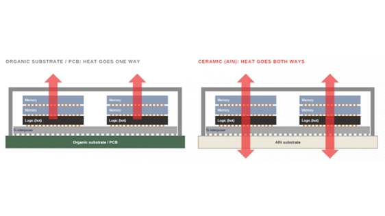
In conventional organic architectures, heat from a logic die generally has a preferred path through the package and toward the cooling system. In a stacked architecture, however, heat-generating logic may sit beneath temperature-sensitive memory or other devices.
That makes thermal management significantly more challenging.
A high-thermal-conductivity ceramic such as AlN can create another path for heat to leave the package. Rather than forcing all the heat through the stack, the substrate can help conduct heat downward and away from the active devices.
AlN’s combination of high thermal conductivity and a CTE relatively close to silicon makes it particularly interesting for these applications.
Ceramic therefore becomes more than a structural component. It can become part of the thermal architecture of the package.
Where This Matters
The same underlying requirements are appearing across several markets.
Aerospace and space systems require compact, lightweight electronics capable of surviving significant temperature changes and demanding operating environments.
Medical devices are pushing toward greater functionality in smaller packages, including MEMS sensing and increasingly complex implantable electronics. Hermeticity, low outgassing, and reliable electrical feedthroughs can become critical packaging considerations.
EVs and power electronics are increasing the use of SiC and GaN as systems move toward higher voltages and greater power density. Thermal management and reliability become increasingly important as these devices operate under demanding electrical and thermal conditions.
AI and high-performance computing are driving another major change: the amount of power being delivered within a package and across a system is increasing rapidly. As power density rises, the package and substrate must increasingly participate in thermal management rather than simply provide electrical interconnection.
Ceramic Is Not Replacing the PCB
The opportunity for ceramic does not mean organic substrates are going away.
PCBs and organic package substrates continue to provide significant advantages in routing density, cost, scalability, and system-level integration. In many designs, the most effective architecture may combine organic and ceramic technologies rather than choosing one exclusively.
The question is where each material provides the greatest value.
For high-power devices, thermally demanding assemblies, hermetic packages, RF applications, and other high-reliability environments, ceramic can address limitations that become increasingly difficult to overcome with conventional organic materials alone.
That makes ceramic substrate development an important consideration earlier in the packaging design process.
From Substrate to System
As heterogeneous integration continues to evolve, the substrate can no longer be viewed simply as the layer connecting a package to a PCB.
It can influence thermal performance, mechanical reliability, electrical behavior, environmental protection, and ultimately the size and architecture of the complete system.
Ceramic substrates have supported high-reliability electronics for decades. What is changing is the range of applications where their advantages are becoming relevant.
For designers working with GaN, SiC, MEMS, RF, medical, aerospace, or other high-reliability technologies, ceramic may provide another path to managing the combination of power density, thermal stress, and integration that next-generation packaging demands.
At Promex, custom substrate design and fabrication is part of a broader advanced microelectronics manufacturing capability, supporting ceramic and other substrate technologies from prototype through production for demanding applications.
As packaging moves beyond the PCB, the substrate itself is becoming an increasingly important part of the solution.
Related Chiplet
- Optical Chiplet
- Reverse Gearbox Chiplet
- FlexGen Multi-Die Smart Network-on-Chip (NoC) IP
- Ncore Multi-Die Interconnect IP
- Integrated voltage regulator (IVR) chiplet
Related Blogs
- Extending Moore’s Law via high-end packaging and advanced IC substrates
- Advanced Packaging Evolution: Chiplet and Silicon Photonics-CPO
- Integrated Design Ecosystem™ for Chiplets and Heterogeneous Integration in Advanced Packaging Technology
- Advanced Packaging Changes the Rules for Semiconductor Health and Performance Management
Latest Blogs
- Ceramic Substrates for Advanced Semiconductor Packaging: Benefits and Applications
- Accelerating Scalable and SI-Aware 2.5D Interconnect Routing with OmniRoute
- The Economics of a Failed Chiplet Package
- Silicon Motherboard Enables Double-Sided Integration of ICs and Passive Components
- The Step-by-Step Process of STCO