Chiplet Modularity Is Becoming Part of the AI Architecture

The chiplet is moving beyond a packaging choice.
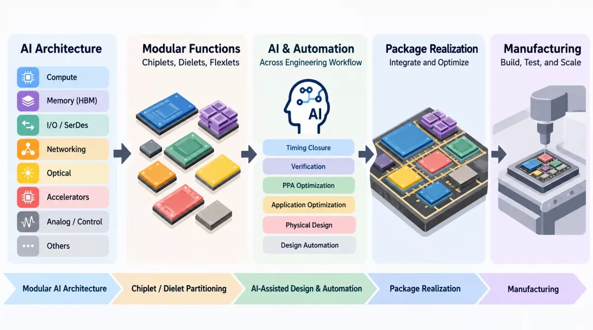
As AI infrastructure becomes more heterogeneous, modularity is increasingly becoming part of the system architecture itself. Compute, memory, high-speed I/O, networking, optical functions, accelerators, control functions, and other specialized capabilities can increasingly be partitioned across chiplets, dielets, flexlets, and other functional building blocks.
At the same time, the engineering workflow used to create those systems is changing.
AI is expanding across semiconductor engineering through timing closure, verification, physical design, PPA optimization, performance optimization, application-aware optimization, and increasingly broader design automation.
These trends reinforce each other.
More modular hardware creates more architectural choices. AI and automation allow more of those choices to be explored. The package then has to physically realize what the architecture creates.
That may become one of the central challenges of the next chiplet era.
The Chiplet Is Becoming Part of Architecture Definition
The original chiplet discussion was often centered on breaking a large monolithic die into smaller pieces.
That remains important, but the direction is becoming broader.
Future heterogeneous AI systems can partition different functions according to the technology that best serves them:
compute → HBM → I/O → SerDes → networking → optical functions → accelerators → analog/control → specialized dielets
The important change is not merely the number of dies.
It is the diversity of the functions being separated.
A compute chiplet may require the most advanced logic technology.
An I/O dielet may optimize for high-speed electrical connectivity.
A memory interface may be driven by bandwidth and proximity to HBM.
An optical function introduces alignment, thermal, and assembly constraints.
Other specialized functions may favor entirely different process technologies, power conditions, or physical locations.
The chiplet therefore becomes part of system partitioning.
The architectural question is increasingly:
Which functions should remain together, which should become separate chiplets or dielets, and where should those functions physically reside?
That makes chiplet architecture and package architecture increasingly difficult to separate.
AI Is Expanding Across the Chip Design Workflow
The design workflow is becoming more modular at the same time.
AI is not entering EDA through one universal system.
Different approaches address different engineering problems.
Some focus on timing closure.
Others focus on verification and debug.
Others address PPA and physical implementation.
Still broader approaches connect multiple engineering tasks through agents, orchestration, and automation.
The flow is moving toward something like:
specialized AI agents → specialized engineering workflows → orchestration → automation → design optimization
This can shorten engineering loops and allow more design alternatives to be evaluated.
That is valuable for chiplet systems because partitioning itself creates a large architectural search space.
Which process should each function use?
How large should each die be?
Where should memory sit?
Where should I/O sit?
What should remain electrical?
What moves toward optics?
What architecture gives the best combination of performance, power, cost, and manufacturability?
AI-assisted engineering can help explore this growing space.
But exploring more architectures does not make them physically easier to build.
Faster Design Creates More Package Decisions
A faster upstream design process can produce more candidate architectures.
But each candidate becomes a physical problem downstream.
A new chiplet creates another interface.
A new dielet creates another placement requirement.
More HBM changes routing, power delivery, and thermal behavior.
Higher-speed I/O changes electrical constraints.
Optical functions introduce alignment and assembly requirements.
Higher compute density changes cooling.
More dies change package size, substrate routing, warpage, assembly sequence, and test strategy.
This leads to an important distinction:
Chiplet modularity can increase architectural flexibility while increasing physical coupling.
The architecture may become easier to compose from specialized functions.
The package must still make all of those functions work together.
More Specialized Chiplets Mean More Specialized Physical Requirements
A heterogeneous package is not simply a collection of smaller dies.
Each chiplet can bring its own physical requirements.
The package may have to reconcile:
bandwidth → latency → signal integrity → power delivery → thermal behavior → mechanical stability → optical alignment → testability → reliability
The more heterogeneous the functions become, the more difficult this reconciliation becomes.
That is why chiplet engineering increasingly extends beyond die-to-die connectivity.
The physical placement of the chiplets matters.
Their relationship to memory matters.
Their power density matters.
Their thermal interaction matters.
Their position relative to optical or electrical I/O matters.
Their assembly sequence matters.
Their test strategy matters.
In other words:
The chiplet may be modular, but its physical behavior is not independent of the system around it.
The Package Becomes the Convergence Point
This is where package realization becomes central to the chiplet architecture.
Many upstream decisions ultimately converge into package geometry.
A compute decision can change HBM placement.
HBM placement can change routing.
Routing can change substrate architecture.
Substrate geometry can affect signal integrity, power delivery, and warpage.
Thermal requirements can change materials, bonding, cooling structures, and mechanical behavior.
Optical integration can introduce entirely new alignment and assembly constraints.
AI-assisted optimization can accelerate decisions upstream.
But eventually those decisions become physical.
AI can accelerate chiplet design and architectural exploration, but it cannot remove the physical constraints created by the resulting architecture.
The package is where those constraints have to coexist.
Automation Expands the Architecture. Realization Narrows It.
This creates an interesting asymmetry.
AI and automation can expand the number of architectures engineers are capable of exploring.
Package realization has to narrow those possibilities to the architectures that can actually be built.
The flow therefore begins to look like:
AI infrastructure requirement
→ modular system architecture
→ chiplet/dielet partitioning
→ AI-assisted design and optimization
→ automation
→ package realization
→ manufacturing
Every stage upstream can create new possibilities.
The last two stages have to determine which possibilities are physically repeatable.
Manufacturing Inherits the Chiplet Architecture
Package realization is still not the end.
Manufacturing has to reproduce the architecture.
A package may work beautifully as a design and still be difficult to build at volume.
More heterogeneous functions can mean tighter placement tolerances, more difficult bonding, additional interfaces, more complex thermal structures, narrower process windows, more inspection, more test, and more complicated yield learning.
So the architecture eventually encounters another question:
Can manufacturing repeatedly build what the chiplet architecture requires?
This is where the implications of modularity become particularly important.
A chiplet architecture is not truly modular if every new combination requires an entirely new manufacturing problem to be solved from the beginning.
The physical interfaces, assembly flows, test methods, and process windows also have to become scalable.
The Next Chiplet Bottleneck May Move Downstream
Chiplets are giving system architects more freedom.
Dielets and specialized functions are increasing that freedom further.
AI-assisted engineering and automation can increase the speed at which architectures are explored and optimized.
All of this is moving the industry forward.
But it can also move the bottleneck.
The difficult question may increasingly shift from:
Can we partition the system?
to:
Can the package physically realize the partition?
and finally:
Can manufacturing reproduce it at scale?
That may define the next stage of chiplet engineering.
As modularity becomes part of AI architecture and AI expands across the engineering workflow, more of the resulting complexity converges at package realization and manufacturing.
The next chiplet era may therefore be determined not only by how intelligently functions are partitioned.
It may be determined by whether the physical realization and manufacturing flow can keep pace with the modular architecture we are creating.
© 2026 Moh Kolbehdari. Original perspective. All rights reserved.
Related Chiplet
- FlexGen Multi-Die Smart Network-on-Chip (NoC) IP
- Ncore Multi-Die Interconnect IP
- Integrated voltage regulator (IVR) chiplet
- High-performance connectivity chiplets
- eFPGA Chiplet
Related Blogs
- OCP Open Chiplet Economy is Leading the Next Wave of AI: Inference
- Inside the Chiplet Revolution: How Arm’s Compute Subsystems Platform is Democratizing Custom AI Silicon
- 2026 Chiplet Summit: Interconnect is the New Frontier of System Performance
- The Chiplet Consolidation Wave: How Strategic Acquisitions are Shaping the Future of Silicon
Latest Blogs
- Chiplet Modularity Is Becoming Part of the AI Architecture
- Hierarchies Of Interconnects Are As Important As Compute And Memory
- UALink over UCIe 3.0: Maximizing Performance for Chiplet-based Designs
- Physical AI Doesn't Just Scale Up. It Scales Out.
- Ayar Labs and GUC Complete Successful Thermal Co-Simulation Testing of Co-Packaged Optics