The Chiplet Is Not the System: Partitioning, Placement, and Package Geometry in Heterogeneous Integration

Party
For years, chiplets have been discussed primarily as a way to partition a large system-on-chip into smaller dies.
That remains important. Partitioning can improve yield, enable IP reuse, allow different functions to use different process technologies, and create more flexible product architectures.
But heterogeneous integration introduces a second question that may become just as important:
Once the functions are partitioned, where should each one physically reside?
Compute, memory, I/O, optical engines, analog functions, power delivery, accelerators, and other specialized dielets may coexist within the same package architecture.
But they do not have the same physical requirements.
Some functions require enormous bandwidth and extremely low latency. Some are sensitive to electrical reach. Some generate significant heat. Others are sensitive to that heat. Some need access to the package edge. Others need the shortest possible path to compute or memory.
The challenge is therefore no longer simply how to divide a design into chiplets.
It is how to partition, place, and physically integrate those functions so that the complete heterogeneous system works.
Logical partitioning determines what the functions are.
Physical partitioning and placement determine where those functions reside.
Package geometry determines whether those functions can operate together as one physical system.
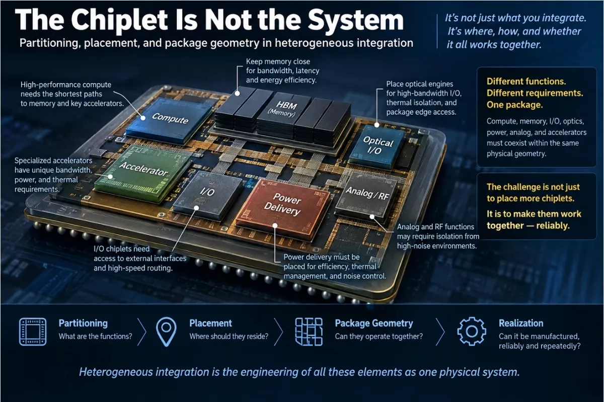
How Local Does Each Function Need to Be?
This creates a deceptively simple architectural question:
How local does each function actually need to be?
The answer is different for every function.
HBM must remain extremely close to high-performance compute because bandwidth, latency, and energy per bit demand tight coupling.
An I/O chiplet has a different locality requirement.
A power-delivery function has another.
An optical engine creates an especially interesting problem. It may benefit from proximity to high-bandwidth electrical interfaces while also requiring consideration of thermal exposure, optical coupling, mechanical alignment, and access to the package boundary.
Other functions may tolerate greater physical separation if doing so improves thermal isolation, manufacturing flexibility, technology optimization, or system scalability.
This means heterogeneous integration is not simply a race to place everything as close together as possible.
Proximity has value, but proximity also has consequences.
The better objective is to place each function at the level of locality its role actually requires.
This idea appeared at a much larger scale in composable infrastructure: resources requiring the greatest bandwidth and lowest latency move inward, while resources that benefit more from capacity, sharing, or flexibility can move outward.
At package scale, the distances are dramatically smaller, but the architectural question remains powerful.
Locality must be engineered.
Package Geometry Becomes Architecture
Once heterogeneous functions occupy a common package, geometry is no longer simply an implementation detail.
Die location.
Die-to-die spacing.
Bump pitch.
Die height.
Bridge, interposer, and RDL geometry.
HBM proximity.
Power-delivery paths.
Optical-engine location.
Thermal paths.
Package edges.
Board transitions.
These are not independent dimensions.
The electrical, optical, thermal, mechanical, and power-delivery paths are different, but they occupy the same physical geometry.
That creates a much harder engineering question:
Where should each function be placed so that electrical, optical, power, thermal, and mechanical requirements can close simultaneously—with reliable functionality?
Consider an electrical path between two dies. Moving them farther apart may increase electrical reach, loss, latency, or power. Moving them closer may improve the electrical interface but increase thermal interaction or constrain routing and assembly.
Moving an optical engine closer to compute may shorten the electrical path but expose the photonic structure to a more difficult thermal environment.
Changing die height can affect mechanical behavior, underfill conditions, assembly, and thermal interfaces.
Changing bump pitch or interconnect density affects not only bandwidth density but manufacturing process windows.
The geometry that improves one domain can make another domain more difficult.
That is why package geometry becomes architecture.
Partitioning and Placement Become Coupled
Traditional design flows can make partitioning appear sequential:
architecture → partitioning → placement → implementation
Heterogeneous integration increasingly makes those decisions interdependent.
A more realistic relationship is:
logical partitioning ↔ physical partitioning ↔ placement ↔ interfaces ↔ package geometry
A logical partition may look attractive until the physical interface required to connect it becomes too expensive in power, area, latency, or routing complexity.
A desirable placement may become problematic once thermal coupling is considered.
An electrical architecture may close nominally but become difficult to manufacture when warpage, registration, bump geometry, assembly tolerances, or material behavior are introduced.
An optical interface may perform well independently but become difficult to maintain once package temperature, mechanical movement, and alignment tolerances are considered.
This is why the physical path matters.
The original system-level formulation extended that path from die through package, board, connector, electrical or optical links, switches, and remote resources. Every boundary adds latency, loss, power, thermal exposure, mechanical variation, manufacturing tolerance, reliability risk, and ultimately system margin.
Within heterogeneous integration, those boundaries become more tightly coupled.
The package is where many of them meet.
Partitioning creates the functional elements. Placement creates their physical relationships. Package geometry determines whether those relationships can close together.
Closing Once Is Not Enough
There is another important distinction.
A heterogeneous package can work once.
That does not necessarily mean it is ready to become a product.
The first objective is functional closure: the electrical, thermal, mechanical, optical, and power-delivery requirements must operate together.
But successful heterogeneous integration ultimately requires more.
The architecture must tolerate manufacturing variation.
Assembly must be repeatable.
Interfaces must remain within their operating margins.
Test access must be considered.
Thermal and mechanical behavior must remain controlled across operating conditions.
Reliability must survive the required product lifetime.
And the resulting system must remain practical to manufacture, qualify, and service.
So the question evolves.
First:
Can all of the physical domains close simultaneously?
Then:
Can they remain closed across manufacturing variation, operating conditions, lifetime, and volume?
This is where heterogeneous integration moves beyond simply placing multiple dies in one package.
It becomes the engineering of a coupled physical system.
The Package Becomes the Physical System
The package was once largely the structure surrounding the semiconductor device.
In heterogeneous integration, that relationship is changing.
The package increasingly determines how compute reaches memory, how dies communicate, how power is delivered, where heat travels, where optical connectivity enters or leaves the system, how mechanical loads are distributed, and how the individual semiconductor functions are physically assembled into a product.
The package therefore cannot be treated simply as a container in which independently designed chiplets are placed.
It becomes the physical architecture in which partitioning, placement, interfaces, and geometry must close together.
This also changes how chiplet architecture should be considered.
The objective is not simply more chiplets.
It is not maximum disaggregation.
And it is not minimum distance everywhere.
The objective is to determine which functions belong together, how local each needs to be, where each should physically reside, and what package geometry allows all of them to operate together reliably.
That is a different definition of heterogeneous integration.
It connects logical architecture directly to physical realization.
And as AI systems combine more compute, HBM, specialized silicon, high-bandwidth I/O, power delivery, and eventually increasingly integrated optical functions, that connection will become more important.
The final architecture may therefore be defined as much by the relationships between dies as by the dies themselves.
Logical partitioning determines what the functions are.
Physical partitioning and placement determine where they reside.
Package geometry determines whether they can operate together.
Heterogeneous integration determines whether they can operate together repeatedly and reliably as one physical system.
© 2026 Moh Kolbehdari. Original technical perspective. All rights reserved.
Related Chiplet
- Optical Chiplet
- Reverse Gearbox Chiplet
- FlexGen Multi-Die Smart Network-on-Chip (NoC) IP
- Ncore Multi-Die Interconnect IP
- Integrated voltage regulator (IVR) chiplet
Related Blogs
- Accelerating Chiplet Integration in Heterogeneous IC Package Designs
- 2026 Chiplet Summit: Interconnect is the New Frontier of System Performance
- SoC and NoC in the Chiplet Era: Understanding Modern SoC Architecture
- The Impact of UCIe on Chiplet Design: Lowering Barriers and Driving Innovation
Latest Blogs
- Cooling Is Becoming Part of the Chiplet Architecture
- When AI Moves the World: Building a Chiplet Standard for Physical AI
- Co-Packaged Optics Moves from Promise to Production Planning
- Co-Packaged Optics Moves from Promise to Production Planning
- Co-Packaged Optics Moves from Promise to Production Planning