Failure Analysis in Transition: An Industry Survey of Challenges, Priorities, and Standardization Needs in Advanced Packaging and Heterogeneous Integration
By Himanandhan Reddy Kottur 1, Nusra Akter Takia 1, Mahamudul Hassan Fuad 1, Istiaq Firoz Shiam 1, Matthew Walsh 2, Navid Asadizanjani 1
1 Department of Electrical and Computer Engineering, University of Florida, Gainesville, FL, USA
2 Florida Semiconductor Engine, Kissimmee, FL, USA
Abstract
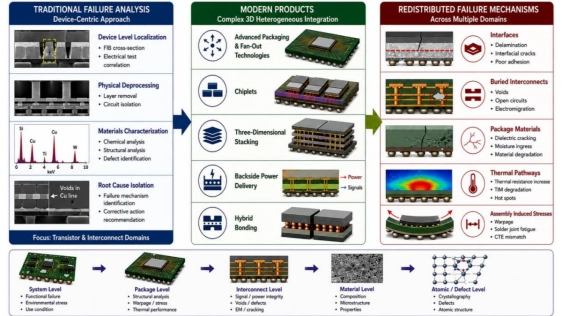
Failure analysis is being reshaped by heterogeneous integration, chiplet-based architectures, hybrid bonding, backside technologies, & increasingly buried package structures. To examine how practitioners view this transition, an anonymous survey was distributed across a broad set of organizations involved in semiconductor design, packaging, systems, tools, & failure analysis. The survey collected approximately one hundred responses & probed organizational background, supported product domains, future priorities in failure analysis, critical bottlenecks, sample preparation challenges, emerging architecture specific pain points, & perceived needs for workflow acceleration & data standardization. The results show that heterogeneous integration, chiplet, and three-dimensional products dominate the respondent base at 69%, while package & heterogeneous integration failure analysis received the highest importance rating at 7.92 out of 10. Hybrid bonding emerged as the most difficult new architecture to analyze at 54%, higher-resolution non-destructive imaging ranked as the most important future accelerator at 8.18 out of 10, and 83% of respondents supported formalized data standardization frameworks. The complete survey data are provided in Appendix A (Table II) to improve transparency & support future benchmarking.
Keywords — failure analysis, heterogeneous integration, advanced packaging, hybrid bonding, chiplets, non-destructive imaging, sample preparation, standardization, artificial intelligence.
To read the full article, click here
Related Chiplet
- Optical Chiplet
- Reverse Gearbox Chiplet
- FlexGen Multi-Die Smart Network-on-Chip (NoC) IP
- Ncore Multi-Die Interconnect IP
- Integrated voltage regulator (IVR) chiplet
Related Technical Papers
- Wafer Warpage of Silicon Interposer in Manufacturing Processes for High Density 2.5D Advanced Packaging: Causes, Measurement, Analysis and Optimization
- High-Bandwidth Chiplet Interconnects for Advanced Packaging Technologies in AI/ML Applications: Challenges and Solutions
- Defect Analysis and Built-In-Self-Test for Chiplet Interconnects in Fan-out Wafer-Level Packaging
- Nanoelectromechanical Systems (NEMS) for Hardware Security in Advanced Packaging
Latest Technical Papers
- Adaptive 3D Chiplet Architecture with Hybrid Wired–Wireless Interconnect for Energy-Efficient Heterogeneous Computing
- LLM-Augmented Bayesian Optimization with Adaptive Policies for Chiplet Design Space Exploration
- Divide and conquer: Scalable performance and energy in MCM GPUs
- A Composable AI-Accelerated Iterative Solver for 3D-IC Thermal Modeling
- QBX: A Compiler for 2-local Qubit Hamiltonian Simulation on Quantum Chiplets