AI-Based Image Enhancement Improves Detection of Interconnect Defects in Microelectronic Packaging
By Raphael Wilhelmer 1, Tatjana Djuric-Rissner 2, Peter Czurratis 2, Hsien-Wei Ho 3, Chun-Hsien Lee 3, Chun-Liang Kuo 3 & Roland Brunner 1
1 Materials Center Leoben Forschung GmbH, Germany
2 PVA TePla Analytical Systems GmbH, Germany
3 Advanced Semiconductor Engineering (ASE) Inc, Taiwan
Abstract
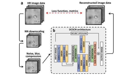
Traditional failure-analysis (FA) methods face growing challenges due to the increasing miniaturization and complexity of modern semiconductor devices. In particular, the detection of cracks in the extreme low K layers of flip-chips, utilized in advanced packaging architectures at the back end of line (BEOL), is challenging. To improve detectability of these so-called “white bumps”, we propose an AI-based image-enhancement workflow, specifically tailored to improve scanning acoustic microscopy (SAM) images. By applying a deep CNN with skip connections and network in network (DCSCN) model to low-resolution C-scan SAM images, we are able to improve the perceptual quality of images. Furthermore, this approach boosts resolution-dependent analysis methods like AI-based object detection of white-bump defects, improving the recall from 5.2% (95% CI: 0.1–26.0%) to 100.0% (95% CI: 82.2–100.0%). Our work demonstrates that AI-based image enhancement can significantly improve FA workflows, offering a robust and efficient solution for modern semiconductor analysis.
To read the full article, click here
Related Chiplet
- Optical Chiplet
- Reverse Gearbox Chiplet
- FlexGen Multi-Die Smart Network-on-Chip (NoC) IP
- Ncore Multi-Die Interconnect IP
- Integrated voltage regulator (IVR) chiplet
Related Technical Papers
- Recent Progress in Structural Integrity Evaluation of Microelectronic Packaging Using Scanning Acoustic Microscopy (SAM): A Review
- Codesign of quantum error-correcting codes and modular chiplets in the presence of defects
- Thermal stability enhancement of low temperature Cu-Cu bonding using metal passivation technology for advanced electronic packaging
- Toward Digital Twins in 3D IC Packaging: A Critical Review of Physics, Data, and Hybrid Architectures
Latest Technical Papers
- AI-Based Image Enhancement Improves Detection of Interconnect Defects in Microelectronic Packaging
- Embodied Emissions of 2.5D and 3D Scaling in Chipletized GPUs for Low-Carbon AI
- Adaptive 3D Chiplet Architecture with Hybrid Wired–Wireless Interconnect for Energy-Efficient Heterogeneous Computing
- LLM-Augmented Bayesian Optimization with Adaptive Policies for Chiplet Design Space Exploration
- Divide and conquer: Scalable performance and energy in MCM GPUs