Thermal Issues Related to Hybrid Bonding of 3D-Stacked High Bandwidth Memory: A Comprehensive Review
By Seung-Hoon Lee, Su-Jong Kim, Ji-Su Lee and Seok-Ho Rhi
Chungbuk National University, Republic of Korea
Abstract
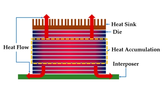
High-Bandwidth Memory (HBM) enables the bandwidth required by modern AI and high-performance computing, yet its three dimensional stack traps heat and amplifies thermo mechanical stress. We first review how conventional solutions such as heat spreaders, microchannels, high density Through-Silicon Vias (TSVs), and Mass Reflow Molded Underfill (MR MUF) underfills lower but do not eliminate the internal thermal resistance that rises sharply beyond 12layer stacks. We then synthesize recent hybrid bonding studies, showing that an optimized Cu pad density, interface characteristic, and mechanical treatments can cut junction-to-junction thermal resistance by between 22.8% and 47%, raise vertical thermal conductivity by up to three times, and shrink the stack height by more than 15%. A meta-analysis identifies design thresholds such as at least 20% Cu coverage that balances heat flow, interfacial stress, and reliability. The review next traces the chain from Coefficient of Thermal Expansion (CTE) mismatch to Cu protrusion, delamination, and warpage and classifies mitigation strategies into (i) material selection including SiCN dielectrics, nano twinned Cu, and polymer composites, (ii) process technologies such as sub-200 °C plasma-activated bonding and Chemical Mechanical Polishing (CMP) anneal co-optimization, and (iii) the structural design, including staggered stack and filleted corners. Integrating these levers suppresses stress hotspots and extends fatigue life in more than 16layer stacks. Finally, we outline a research roadmap combining a multiscale simulation with high layer prototyping to co-optimize thermal, mechanical, and electrical metrics for next-generation 20-layer HBM.
Keywords:
3D-stacked memory; High-Bandwidth memory (HBM); hybrid bonding; thermal management; metal density
To read the full article, click here
Related Chiplet
- Integrated voltage regulator (IVR) chiplet
- High-performance connectivity chiplets
- eFPGA Chiplet
- DPIQ Tx PICs
- IMDD Tx PICs
Related Technical Papers
- On-Package Memory with Universal Chiplet Interconnect Express (UCIe): A Low Power, High Bandwidth, Low Latency and Low Cost Approach
- Probing the Nanoscale Onset of Plasticity in Electroplated Copper for Hybrid Bonding Structures via Multimodal Atomic Force Microscopy
- Thermal stability enhancement of low temperature Cu-Cu bonding using metal passivation technology for advanced electronic packaging
- High-Efficient and Fast-Response Thermal Management by Heterogeneous Integration of Diamond on Interposer-Based 2.5D Chiplets
Latest Technical Papers
- DICE: Detailed Inter-Chiplet End-to-End PHY Modeling for Accurate Chiplet Simulation
- APEX: an Adaptive Photonic-Electronic Chiplet Interconnection Architecture for DNN Inference
- Formal Foundations for Known Good Reliable Die Screening in Chiplet-Based AI Systems-on-Chip
- Optimization of Test-Access Architectures and Test Scheduling for 2.5D/3D Integration
- Learning to Place Chiplets: A Multi-Objective Reinforcement Learning Approach