JCET Advances High-Aspect-Ratio TSV Technology for 2.5D and 3D Packaging
August 19, 2026 – JCET today announced a significant advance in its high-aspect-ratio through-silicon via (TSV) technology, following the successful fabrication of samples in collaboration with its partners.
Developed for 2.5D and 3D advanced packaging, silicon interconnects, and multidimensional heterogeneous integration, JCET’s TSV process strengthens a critical component of the company’s microsystem integration platform. The technology is intended to support more complete and flexible manufacturing solutions for the system-level integration of high-performance computing and memory devices.

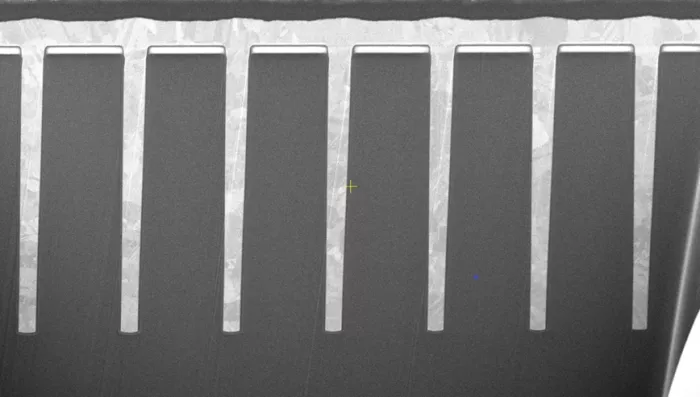
Cross-Sectional Image of a High-Aspect-Ratio TSV Sample
The sample fabrication incorporated several critical process steps, including deep silicon etching, sidewall dielectric deposition, barrier and seed layer deposition, and copper filling. The fabricated TSVs measured 1.5 micrometers in diameter and 17 micrometers in depth, achieving an aspect ratio of 11.3:1. The results demonstrate JCET’s advanced process development and joint validation capabilities for small-diameter, high-aspect-ratio TSVs.
Rapid growth in artificial intelligence, high-performance computing, and high-bandwidth memory is driving demand for interconnects that offer greater density, lower electrical loss, and improved reliability. These interconnects are essential for integrating GPUs, ASICs, HBM, and other functional chiplets within increasingly complex systems.
TSVs create vertical electrical connections through a silicon wafer or die and are a fundamental enabling technology for 2.5D and 3D integration, vertical die stacking, and heterogeneous Chiplet integration. Developing high-aspect-ratio TSVs requires precise control across a series of tightly integrated wafer-level processes, with the performance of each step directly affecting the overall process flow.

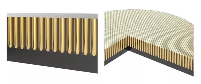
Schematic Illustration of a TSV
The successful sample fabrication expands JCET’s R&D capabilities in wafer-level advanced packaging and silicon interconnects. It also provides a foundation for integrating TSV formation with redistribution layers and related wafer-level processes as JCET continues to develop end-to-end silicon interposer manufacturing capabilities.
The ability to form TSVs on incoming customer wafers will allow JCET to more closely connect wafer-level processing, silicon interconnects, and system integration. It will also provide greater flexibility in integrating chiplets manufactured at different process nodes and designed for different functions and system architectures.
High-aspect-ratio TSV technology is designed to support two primary advanced packaging applications. The first is 3D stacked integration, in which TSVs formed in the underlying wafer or die create vertical electrical connections between stacked devices. The second is silicon-based interconnect structures, including silicon interposers. When integrated with redistribution layers, micro-bumps, and wafer-level packaging processes, TSVs can provide critical process support for 2.5D integration, multi-chiplet interconnects, and HBM integration.
Dr. Rebecca Chen, Vice President of JCET and General Manager of the AI & Smart Industry BU, said: “This progress in high-aspect-ratio TSV technology marks an important step in expanding JCET’s advanced packaging capabilities. We will follow a disciplined path from technology development and engineering validation to volume production, while strengthening critical process technologies and integrating them into a more complete end-to-end manufacturing platform.”
Related Chiplet
- Optical Chiplet
- Reverse Gearbox Chiplet
- FlexGen Multi-Die Smart Network-on-Chip (NoC) IP
- Ncore Multi-Die Interconnect IP
- Integrated voltage regulator (IVR) chiplet
Related News
- imec: New Methods for 2.5D and 3D Integration
- Onshoring Advanced Packaging Update
- Siemens and Intel Foundry advance their collaboration to enable cutting-edge integrated circuits and advanced packaging solutions for 2D and 3D IC
- Advanced IC Packaging: The Roadmap to 3D IC Semiconductor Scaling
Latest News
- Amkor Technology and NVIDIA Advance Strategic Partnership for AI Infrastructure
- Siemens expands agentic AI collaboration to tackle 3D IC power and thermal challenges with NVIDIA
- Photon Bridge Raises €10M to Tackle AI’s Emerging Laser Bottleneck
- Abacus Semiconductor and Aalto University Announce Research Cooperation on High-Speed Chiplet Interconnects
- UK Launches Semiconductor Catapult to Strengthen Sovereign Capabilities in AI Hardware and Defence