The Next Chiplet Era: Compute Meets Optical Chiplets

The first phase of the chiplet era was largely about partitioning silicon.
Instead of building every function on one increasingly large monolithic die, designers could separate compute, memory, I/O, acceleration, and other functions into optimized dies and reconnect them inside an advanced package. That shift changed semiconductor economics, yield strategy, process-node selection, and system architecture.
The next phase may change something equally fundamental:
where electrical communication ends and optical communication begins.
Optical chiplets are moving photonic functionality progressively closer to compute. That movement is often described simply as a response to the limitations of electrical interconnects: copper becomes increasingly difficult to scale in bandwidth, reach, and power, so optics must move inward.
That description is directionally correct, but incomplete.
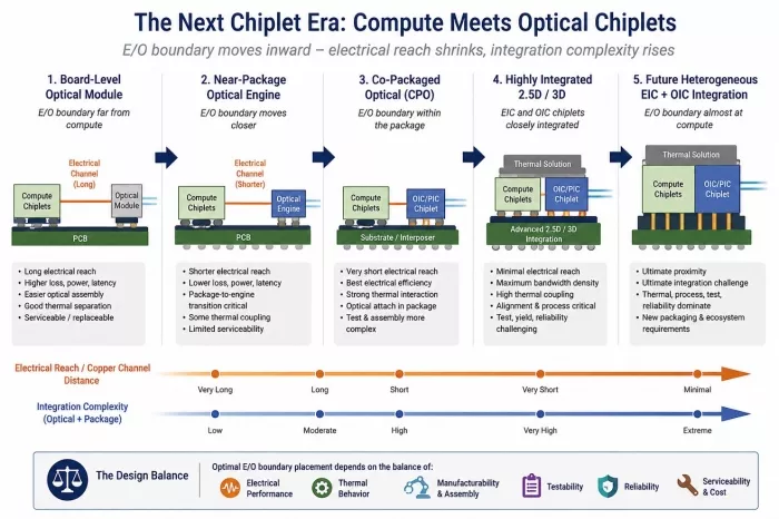
The future heterogeneous package will not simply replace electrical with optical. It will continuously rebalance electrical reach, optical proximity, thermal exposure, package complexity, manufacturability, testability, reliability, and serviceability as electronic and optical chiplets move closer together.
That makes optical chiplets more than a new I/O technology.
They introduce a new partitioning problem for the chiplet ecosystem itself.
The E/O Boundary Is Becoming a Design Variable
In conventional systems, the electrical-to-optical conversion boundary was relatively far from the compute silicon. High-speed electrical signals traveled through the package, across significant portions of the PCB, through connectors and into pluggable optical modules.
As bandwidth has increased, that electrical distance has become progressively more expensive.
Higher-frequency channels increase insertion loss and crosstalk sensitivity. Equalization and retiming consume additional power. PCB routing becomes more difficult. Connector launches consume channel margin. The energy required simply to transport bits from the processor to the optical module becomes increasingly significant.
The industry's response is already visible in the progression from board-level optics toward near-package optics and co-packaged optics. Recent work describes 2D, 2.5D, and 3D heterogeneous approaches that increasingly combine electronic ICs and photonic ICs, while identifying thermal management, manufacturability, and standardization as major remaining challenges.
This creates a new architectural question:
Where should the electrical-to-optical transition actually occur?
Move the optical engine closer to compute and the electrical channel becomes shorter.
That can reduce loss, latency, routing congestion, equalization burden, and electrical energy per bit.
But every step inward creates a different set of problems.
The optical engine is exposed to a more difficult thermal environment. Fiber attach becomes a package-integration issue. Mechanical tolerances become coupled to optical performance. Test must span electrical and optical domains. Known-good-die strategy becomes more complicated. Repair and serviceability change. Package yield increasingly depends on components produced through different technologies and potentially different suppliers.
At some point, EIC–OIC proximity stops being merely a channel problem and becomes an integration problem.
That transition will shape the next generation of chiplet architectures.
Optical Chiplets Change the Meaning of Partitioning
Traditional chiplet partitioning asks questions such as:
- Which function belongs on which process node?
- Which dies should be reused across products?
- How much bandwidth is required between chiplets?
- Which functions should be tightly coupled?
- Which interfaces should be standardized?
Optical chiplets add another question:
Which communication should remain electrical, and where should the system transition into the optical domain?
That decision affects far more than the optical link.
Consider the spectrum of possible implementations.
At one end, optics remains relatively remote. This preserves easier optical assembly, thermal separation, replacement, and serviceability—but leaves the system with a longer high-speed electrical path.
Move the optical engine closer to the package and the electrical reach decreases. The system gains electrical margin, but packaging and thermal interactions increase.
Move the photonic and electronic functions into the same heterogeneous package and the electrical distance can become extremely small. But now the package must simultaneously close electrical, optical, thermal, mechanical, manufacturing, test, and reliability constraints.
There is therefore no universal answer that says closer is always better.
The optimum location of the optical chiplet depends on the system.
The Electrical Corridor Does Not Disappear
There is another consequence that is easy to overlook.
As optics moves closer to compute, the remaining electrical connection becomes shorter—but more architecturally important.
That electrical segment may carry enormous bandwidth density directly between the compute/SerDes domain and the optical engine. It cannot always be treated as ordinary package escape routing.
Instead, it increasingly becomes a controlled transport corridor.
Its geometry, reference continuity, crosstalk environment, manufacturing tolerance, and electrical-to-optical handoff must be designed together with the package.
This creates an interesting evolution.
Long electrical channels place enormous emphasis on equalization and channel compensation.
Near-package optics shortens the channel, but concentrates the importance of the package-to-optical-engine transition.
Highly integrated optical chiplets shorten the electrical segment further, but now thermal and assembly interactions increasingly dominate.
The problem does not disappear as the corridor gets shorter.
The dominant constraint changes.
That is an important distinction for chiplet architects.
Why This Matters Now
This is no longer purely a research trajectory.
Commercial and ecosystem activity is beginning to make optical chiplets part of the practical AI interconnect discussion. Lightmatter, for example, reported sampling of a co-packaged-optics chiplet delivering 1.6 Tb/s per fiber and has announced both CPO and NPO participation in the NVIDIA NVLink Fusion ecosystem.
Meanwhile, a multi-company initiative within the Open Compute Project is developing a shared CPO system architecture intended to support interoperable silicon-photonics infrastructure for AI systems.
This matters because chiplets only become an ecosystem when interfaces and responsibilities become sufficiently clear for different participants to build different pieces.
That same transition occurred for electrical chiplets.
UCIe has progressively expanded the concept of an interoperable package-level ecosystem, with UCIe 3.0 now supporting 48 and 64 GT/s operation and broader multi-chip system topologies.
Optical chiplets introduce an additional dimension to that ecosystem.
Interoperability will eventually need to encompass not only digital protocols and die-to-die interfaces, but also questions surrounding optical engines, electrical interfaces to those engines, thermal environments, fiber attachment, test access, package assembly, and lifecycle management.
In other words, the ecosystem challenge expands from:
Can these chiplets communicate?
to:
Can these electronic and optical chiplets be integrated, manufactured, tested, qualified, and serviced together?
From Chiplet Connectivity to Heterogeneous Transport Architecture
The next chiplet era may therefore be defined less by adding another type of die and more by changing the role of the package.
The package becomes the place where the system decides:
how long electrical transport should remain electrical,
where optical conversion should occur,
how closely EIC and OIC should be coupled,
and which integration penalties are acceptable to gain that proximity.
Different systems will reach different answers.
Some architectures will continue to benefit from pluggable optics.
Others will move the optical engine near the package.
Some will adopt co-packaged optics.
And increasingly aggressive systems may push toward much tighter 2.5D and 3D heterogeneous integration of electronic and photonic chiplets.
These are not simply competing technologies. They are points along an evolving electrical–optical partitioning continuum.
The important engineering challenge is understanding what changes as that boundary moves.
Electrical reach decreases.
Optical integration increases.
And somewhere between those trends lies the architecture that provides the right balance of bandwidth, power, thermal behavior, manufacturability, reliability, testability, and serviceability for a particular system.
The Next Chiplet Question
The first chiplet revolution asked:
What should remain on one die, and what should become a chiplet?
The optical-chiplet era adds another question:
Where should electrical transport end and optical transport begin?
That question reaches far beyond photonics.
It changes package architecture, chiplet placement, electrical interfaces, thermal design, manufacturing flows, test strategy, and ultimately the way heterogeneous systems are partitioned.
That is why optical chiplets may represent more than the next interconnect technology.
They may help define the next architecture of the chiplet itself.
Related Chiplet
- FlexGen Multi-Die Smart Network-on-Chip (NoC) IP
- Ncore Multi-Die Interconnect IP
- Integrated voltage regulator (IVR) chiplet
- High-performance connectivity chiplets
- eFPGA Chiplet
Related Blogs
- OCP Open Chiplet Economy is Leading the Next Wave of AI: Inference
- Advancing High‑Performance Silicon Photonics and Silicon Germanium (SiGe) for the Next Era of Optical Connectivity
- Addressing the Colossal Challenge of System Co-Optimization with a Holistic Chiplet Design Methodology
- Enabling the Chiplet Era
Latest Blogs
- Chiplet Modularity Is Becoming Part of the AI Architecture
- Hierarchies Of Interconnects Are As Important As Compute And Memory
- UALink over UCIe 3.0: Maximizing Performance for Chiplet-based Designs
- Physical AI Doesn't Just Scale Up. It Scales Out.
- Ayar Labs and GUC Complete Successful Thermal Co-Simulation Testing of Co-Packaged Optics