Accelerating Chiplet Integration in Heterogeneous IC Package Designs

Today’s multi-chip and chiplet solutions are leading the way for the “More than Moore” vision, with companies leveraging packaging technologies to create value and differentiation from their competitors. Silicon via (TSV), wafer-level packaging (WLP), and 3D stacking technologies are providing a tremendous number of packaging options for all form factors. The figure below provides a common example of 3D die/wafer stacking vs. the traditional 2D system on a chip (SoC).

As semiconductor packaging technologies such as chip-on-wafer-on-substrate with redistribution layer (CoWoS-R) and CoWoS local silicon interconnect (CoWoS-L) increase in complexity due to the rapid growth in the number of signals and high-bandwidth memory (HBM) memory integration, high-speed interface areas are a key focus for design and analysis. This complexity challenges traditional design and analysis workflows, as importing large designs into analysis tools and managing redesigns can exceed project time constraints, making it difficult to meet deadlines.
In response to these challenges, Cadence has developed a novel methodology that enables early and iterative optimization of IC package designs. This approach eliminates the need to wait for complete designs or spend excessive time preparing simulations. By integrating in-design analysis and optimization with Cadence’s scalable multiphysics analysis engines, IC package engineers can accelerate design cycles and efficiently improve complex package design efficiently.
Accelerating Chiplet Integration in Heterogeneous IC Package Designs, an on-demand webinar presented by Cadence’s Mark Gerber, Brad Griffin, and Gary Lytle, covers early-stage design optimization that eliminates the need to wait for full design completion. This is done by reducing simulation preparation time through a methodology of rapidly iterating and enhancing designs to align with project management expectations and leveraging scalable multiphysics analysis engines for comprehensive package design evaluation and signoff.
Advanced Packaging Key Challenges and Cadence Solutions
Cadence offers a variety of solutions to address the design challenges of new IC package structures:
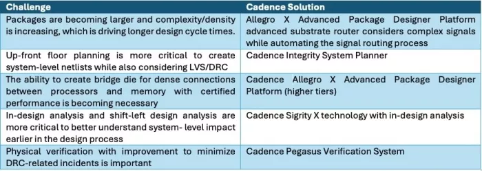
In summary, as packaging design has become more complicated, Allegro X Advanced Package Designer Platform continues to lead the IC packaging design community. Cadence design technology has evolved quickly to support 3D planning, silicon bridges, in-design analysis, automated substrate routing, and physical verification (LVS).

Design and Analysis Flow
Constraint-driven design streamlines development and reduces costs, strategic floor planning shortens cycles and lowers expenses, and automated routing speeds workflows and cuts manual work. In-design analysis enables early electrical/thermal issue detection and accelerates signoff and selective design cutting saves engineering time and enables parallel problem-solving.
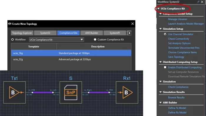
An example of this flow, covered in the webinar, is a 16Gbps Universal Chiplet Interconnect Express (UCIe) interface with ground trace shielding. The analysis team was tasked with finding the optimal constraints to guide routing, and the routing team needed to implement the routing patterns to meet the constraints. A methodology is reviewed where stringent spacing and shielding is required for longer connections and tighter spacing with less shielding can be used for shorter connections.

The UCIe compliance kit in Sigrity X SystemSI provided guidance on which routing configurations could be used to meet the UCIe electrical requirements. The UCIe interface compliance kit within the Sigrity X topology workbench is shown below.
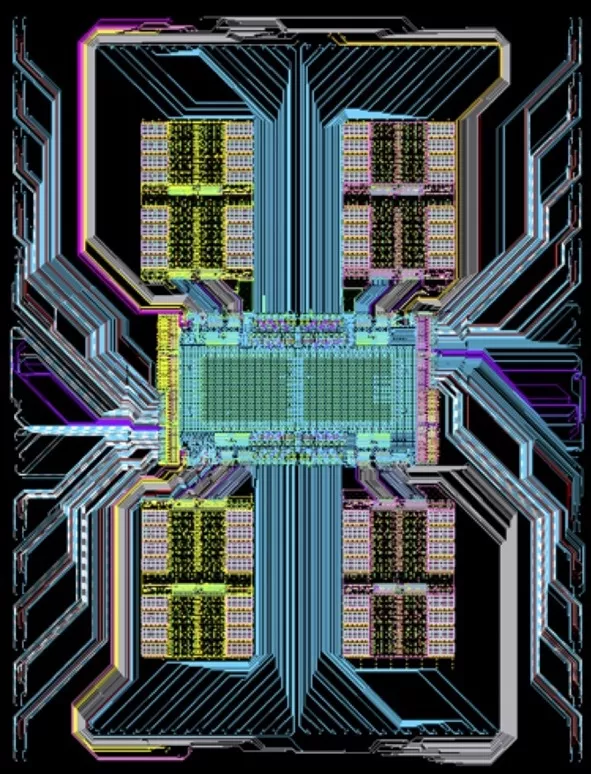
The bottleneck for advanced package design is routing. Cadence’s advanced substrate router technology (shown below) provides an optimized automated routing flow for 3D-IC design to streamline substrate layout generation. It optimizes the routing of high-density die-to-die and die-to-substrate connections and provides multi-core performance benefits. This technology supports diverse requirements for any angle routing, auto shielding, bus breakout routing, high-density bump escape planning, differential pair routing, and fillet/teardrop insertion for yield improvement.
IC Package Analysis and Signoff
The following figure shows how Sigrity X and Clarity 3D Solver work together to provide advanced IC package signal integrity analysis and signoff.
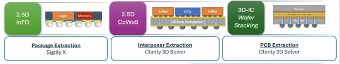
Three platforms comprise the complete flow: Allegro X Advanced Package Designer Platform, Sigrity X, and Clarity 3D Solver. Together, they allow exploration, in-design analysis, and signoff, including spec-driven compliance reports.
A case study within the webinar demonstrates and provides results for a full 3D extraction of an interposer with Clarity, as well as Sigrity X SystemSI simulation results with the interposer model.
Conclusion
Times have changed and manual-driven design workflows used with yesterday’s IC package designs lack the efficiency required to address electrical, thermal, and mechanical challenges of modern 3D package design. Cadence offers a modern flow that meets the latest design requirements, enabling multi-chip(let) solutions that are leading the way for a “More than Moore” vision. Chip companies are leveraging TSV, WLP, and 3D stacking packaging technologies to create value and differentiation and provide a tremendous number of packaging options for all form factors.
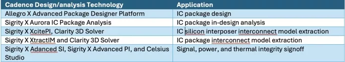
This blog summarizes the Accelerating Chiplet Integration in Heterogeneous IC Package Designs webinar, which presents some of the revolutionary solutions Cadence offers that enable IC companies to create the leading-edge products of the future (see below table). Click here to learn more and view this valuable webinar on demand.
You can learn more about Allegro X Advanced Package Designer Platform here, Sigrity X here, and Clarity 3D Solver here. You can also learn more about Cadence chiplet design solutions by downloading our eBook, “Helping You Realize Your Chiplet Ambitions.”
Related Chiplet
- eFPGA Chiplet
- DPIQ Tx PICs
- IMDD Tx PICs
- Near-Packaged Optics (NPO) Chiplet Solution
- High Performance Droplet
Related Blogs
- Accelerating the AI Economy through Heterogeneous Integration
- How to Streamline Your Advanced Package (Chiplet, 3DIC) Interconnect Designs
- Demystifying 3D ICs: A practical framework for heterogeneous integration
- Chiplet Integration in the Automotive Realm
Latest Blogs
- How Intel Foundry Packaging Technologies Redefine AI and HPC Scalability Limits at ECTC 2026
- From complexity to simplicity: Scaling and future-proofing chiplets with AMBA®︎ CHI C2C property negotiation
- High-Speed Heterogeneous Integration with Multiphysics Analysis for TSMC SoW-X
- Chiplet Realization Beyond the Package: Why the Next AI Bottleneck Moves to the Interposer-to-PCB Boundary
- Advancing UCIe Performance: Enabling 40G for Next-Generation Multi-Die Designs